Low-power dual op-amp for battery-powered signal conditioning
The CMOS input stage delivers an input bias current of 0.6 pA, which keeps leakage from corrupting high-impedance sources such as photodiode or pH probe front-ends.
It is sized for low-frequency conditioning — think DC to a few kilohertz at most. A unity-gain buffer handling a 1 kHz, 1 Vpp sine wave will slew without distortion, but a 10 kHz signal at the same amplitude exceeds the slew limit. For a thermocouple amplifier with a 10 Hz bandwidth or a strain-gauge bridge running at 100 Hz excitation, the 110 kHz GBW leaves ample loop gain for precision. The trade-off is clear: you trade bandwidth for the 20 µA supply draw.
The 1.1 mV typical input offset voltage is adequate for 8- to 10-bit systems without auto-zero; for higher resolution, a trim or a chopper-stabilized part would be needed.
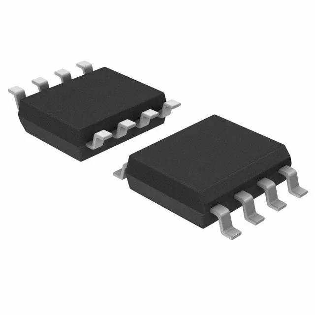
The SOIC-8 footprint is standard and matches the vast majority of dual op-amp layouts. For a 20 µA part, thermal management is not a concern even at elevated ambient.