Dual CMOS op-amp in a through-hole DIP — what the 2.2 MHz GBW and 0.7 pA bias mean for your signal chain
The 0.7 pA typical input bias current makes it a strong fit for high-impedance sources like photodiode transimpedance stages or pH probe buffers where JFET or CMOS inputs are required to avoid loading the source. The 1.9 mA total quiescent current (both channels) keeps the power budget modest — about 6.3 mW at 3.3 V, 30 mW at 16 V.
This limits deployment to temperature-controlled environments: lab instruments, office peripherals, consumer audio, test equipment, and similar indoor gear. It is not qualified for automotive under-hood, outdoor telecom cabinets, or industrial motor drives where ambient temperatures routinely exceed 70°C or drop below freezing. If your application needs extended temperature, look at the TLC277's industrial-grade siblings (e.g., TLC277IP, -40°C to 85°C) or the surface-mount TLV series alternatives.
8-DIP through-hole — prototyping ease vs. production density
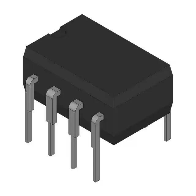
The 8-pin DIP package (0.300" row spacing, 7.62 mm body width) is a through-hole format. It is straightforward to hand-solder, socket, and rework — a clear advantage for breadboard prototyping, one-off builds, and legacy board repairs. In volume production, however, through-hole adds insertion cost and consumes more board area than a surface-mount SOIC-8 or MSOP-8. If your BOM targets automated assembly or high density, the TLC277 is also available in SOIC-8 (TLC277CD) and other SMD variants.
The part is RoHS3 compliant (lead-free) and remains in regular production. For dual-sourcing or a surface-mount alternative, the TLV9352 (10.6 MHz, rail-to-rail output) or OPA4374 (6.5 MHz, quad channel) are functional peers in different package and performance tiers — but neither is a direct pin-for-pin drop-in for the DIP footprint.