The 2.25 MHz gain-bandwidth product and 3.6 V/µs slew rate suit it for audio-frequency signal conditioning, active filters below 100 kHz, and control-loop buffering in industrial sensors, bench instruments, and commercial-grade test gear.
Supply range and single-supply operation
The TLC2274CN operates from a single supply as low as 4.4 V up to 16 V, or from split supplies of ±2.2 V to ±8 V. The rail-to-rail output stage swings within millivolts of each rail, so a 5 V single-supply design can deliver a 0.1 V to 4.9 V output swing without an external level shifter. The 4.8 mA total quiescent current (1.2 mA per amplifier) keeps the thermal budget modest in a DIP package, though the 50 mA per-channel output current limit should be derated for continuous drive above 25°C ambient.
Input characteristics for high-impedance interfaces
With a typical input bias current of 1 pA and an input offset voltage of 300 µV, the TLC2274CN can buffer signals from high-impedance sources such as photodiodes, pH probes, or piezoelectric sensors without loading the source.
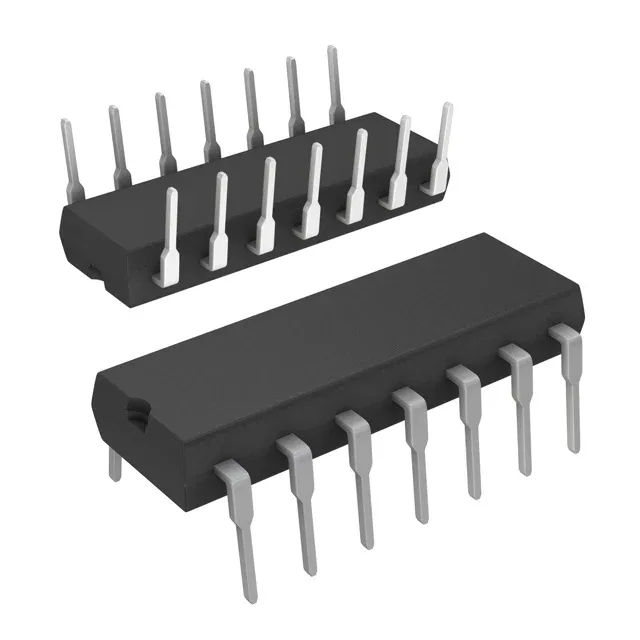
The 14-DIP (0.300" body) is a through-hole package intended for socketed or wave-soldered assembly. The 7.62 mm row spacing is standard for DIP-14 sockets. The tube shipping medium (25 or 50 pieces per tube, depending on distributor pack) is typical for DIP devices; no moisture sensitivity level (MSL) rating applies to hermetic DIPs, so no bake-out is required before soldering. For a rework lab or repair bench, this package is straightforward to hand-solder or replace with a standard DIP extractor.
It is ROHS3 compliant. For dual-sourcing or a surface-mount alternative, the TLV9351IDCKR (single-channel, 3.5 MHz, 20 V/µs) or OPA4374AIPWT (quad, 6.5 MHz, 5 V/µs) offer higher bandwidth in smaller packages, but neither is a drop-in replacement for the DIP-14 footprint.