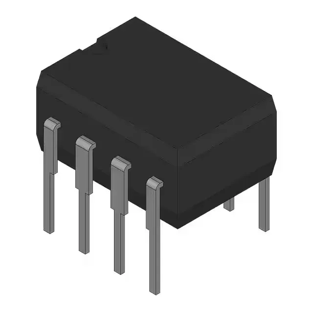
Texas Instruments TL061CJG — Logic ICs

TL061CJG JFET Op-Amp, 1 MHz GBW, 3.5 V/µs, 8-CDIP

MPNTL061CJG
End of Life

Texas Instruments TL061CJG, JFET-input operational amplifier, 1 MHz gain bandwidth, 3.5 V/µs slew rate, 200 µA supply current, 30 pA input bias, single channel, 8-CDIP (0.300", 7.62mm) through-hole package, 0°C to 70°C operating temperature.

$1.84Ref. price · indicative, final on quote
Packaging8-CDIP (0.300", 7.62mm)
StockContact for availability
MOQ1 pcs
  • 100% new & originalTraceable channels only — no refurbs, no pulls, no remarked parts.
  • Date & lot codes on quoteStated per line before you commit; label photos on request.
  • MSL-compliant ESD packingMoisture-sealed bags with indicator cards; reels photo-verified.
  • PayPal buyer protectionPay by T/T, PayPal or Payoneer — card payments covered end to end.

Specifications

TL061CJG Technical Specifications
ParameterValue
Mounting typeThrough Hole
Amplifier typeJ-FET
Voltage - input offset3 mV
Voltage - supply span30 V
Current - supply200µA
Current - input bias30 pA
Operating temperature0°C ~ 70°C (TA)
Gain bandwidth product1 MHz
PackageBulk
Slew rate3.5V/µs
Case8-CDIP (0.300\", 7.62mm)
Number of circuits1

Product details

It delivers a 1 MHz gain-bandwidth product with a 3.5 V/µs slew rate while drawing only 200 µA of supply current. The JFET input stage provides 30 pA typical input bias current, making it suitable for high-impedance signal conditioning, precision integrators, and low-level sensor amplification in temperature-controlled environments (0°C to 70°C).

The TL061CJG operates from a total supply span of 10 V to 30 V, which means it can run on ±5 V to ±15 V dual supplies or a single 10 V to 30 V rail. The 200 µA typical quiescent current keeps the power dissipation low — useful in multi-channel boards where thermal budget is tight. For a ±15 V supply, the total draw is about 6 mW per amplifier, so a dozen of these on a card still stay under 75 mW of op-amp quiescent loss.

The 8-CDIP (0.300", 7.62mm) is a through-hole ceramic dual-in-line package. It is not compatible with standard lead-free reflow profiles — the package body is hermetic, but the leads are tin/lead solder-dipped (RoHS non-compliant per). For new designs, this means hand-soldering or wave-solder assembly only, and the board must accept leaded solder. If you are retrofitting a legacy board that originally used a plastic DIP, the pinout is the same, but the 0.300" width matches standard 8-pin DIP sockets.

Lifecycle and sourcing — active but niche

However, the CDIP package and RoHS non-compliant finish limit its production volume — it is not a high-volume surface-mount part. Expect availability through independent distribution rather than factory-direct in large tape-and-reel quantities. If your design can tolerate a plastic DIP or SOIC package, the commercial-grade TL061 variants (e.g., TL061CP) share the same electrical specs and are more readily stocked.

Frequently asked questions

What is the gain bandwidth of TL061CJG?

The TL061CJG has a gain-bandwidth product of 1 MHz. This sets the small-signal bandwidth at unity gain; for closed-loop gains above unity, the usable bandwidth is 1 MHz divided by the noise gain. For example, at a gain of 10, the -3 dB bandwidth is approximately 100 kHz.

Is TL061CJG equivalent to TL061BCP?

The TL061BCP is the plastic DIP version of the same JFET op-amp die. Electrically, both share the same 1 MHz GBW, 3.5 V/µs slew rate, 200 µA supply current, and 30 pA input bias. The difference is the package: TL061CJG is the 8-CDIP hermetic ceramic (through-hole), while TL061BCP is the 8-PDIP plastic. The CJG suffix indicates the ceramic package, which is RoHS non-compliant and intended for high-reliability or legacy designs. If your board accepts a plastic DIP and does not require hermetic sealing, the BCP is a direct functional equivalent.