Texas Instruments SN74S175D — Analog & Data Acquisition

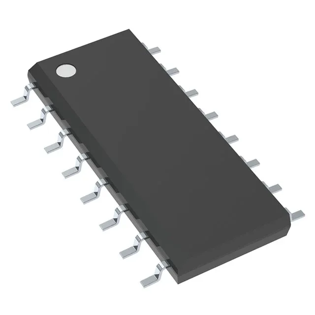
SN74S175D D-Type Flip-Flop, 110 MHz, 16-SOIC

MPNSN74S175D
End of Life

Texas Instruments 74S series SN74S175D, D-Type flip-flop, single element 4-bit, positive edge trigger, complementary output, master reset, 110 MHz clock, 12ns @ 5V/15pF propagation delay, 4.75-5.25V supply, 0°C to 70°C, 16-SOIC surface mount.

$2.89Ref. price · indicative, final on quote
Packaging16-SOIC (0.154", 3.90mm Width)
StockContact for availability
MOQ1 pcs
  • 100% new & originalTraceable channels only — no refurbs, no pulls, no remarked parts.
  • Date & lot codes on quoteStated per line before you commit; label photos on request.
  • MSL-compliant ESD packingMoisture-sealed bags with indicator cards; reels photo-verified.
  • PayPal buyer protectionPay by T/T, PayPal or Payoneer — card payments covered end to end.

Specifications

SN74S175D Technical Specifications
ParameterValue
TypeD-Type
Series74S
Output typeComplementary
Trigger typePositive Edge
Mounting typeSurface Mount
Voltage4.75V ~ 5.25V
Current - quiescent96 mA
Current - output high, low1mA, 20mA
Frequency110 MHz
Operating temperature0°C ~ 70°C (TA)
PackageTube
FunctionMaster Reset
Case16-SOIC (0.154\", 3.90mm Width)
Number of elements1
Number of bits per element4
Max propagation delay @ v, max CL12ns @ 5V, 15pF

Product details

110 MHz clock — what it buys you in a 5V synchronous bus

The Texas Instruments SN74S175D is a 74S-series D-type flip-flop that clocks at 110 MHz with a propagation delay of 12ns at 5V driving 15pF. That puts it in the fast lane of the 5V logic families — well ahead of the 74LS series (40 MHz, 25ns) and competitive with 74F (80 MHz, 10ns). It is a single-element, 4-bit positive-edge-triggered register with complementary outputs and an asynchronous master reset. The 4.75V to 5.25V supply range matches legacy 5V TTL rails, and the 96 mA quiescent current reflects the Schottky-clamped speed advantage.

Master reset and complementary outputs — the logic interface

The master reset input (active low, per the function) clears all four flip-flops asynchronously, which is useful for power-on initialization or emergency reset without waiting for a clock edge. Complementary outputs give you both Q and /Q on each bit — handy for differential data paths or driving paired logic without external inverters. The output drive capability is 1 mA sourcing and 20 mA sinking, typical for Schottky TTL and sufficient for driving one or two standard TTL loads or a CMOS input with a pull-up.

If your design lives in an unconditioned enclosure or sees ambient above 70°C, you will need to budget for airflow or move to an extended-temperature logic family.

It is ROHS3 compliant.

Frequently asked questions

Will SN74S175D drop into a board originally built with SN74LS175NS?

Functionally yes — both are 4-bit D-type flip-flops with positive-edge trigger, complementary outputs, and master reset, in a 16-pin SOIC footprint. The key difference is speed: the 74S part clocks at 110 MHz with 12ns propagation delay, versus 40 MHz and 25ns for the 74LS. The 74S also draws roughly 5x the quiescent current (96 mA vs ~18 mA). If the original board was designed for the slower 74LS timing, the SN74S175D will work, but the higher supply current may exceed the existing power budget. Verify the 5V rail can deliver the extra current before substituting.

What compliance documentation does TI provide for SN74S175D?

The part is ROHS3 compliant. TI typically provides a Declaration of Compliance and material composition data for this series upon request. No UL or IEC certification is listed in the standard catalog data for this logic family.