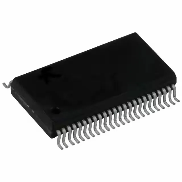
What this 74LVTH buffer does on the bus
It packs four 4-bit elements with non-inverting outputs, each gated by independent output-enable pins, and all outputs go to high-impedance (3-state) when deasserted. The 48-pin TFSOP (TSSOP) footprint is a common fine-pitch surface-mount package, so it fits into existing PCB layouts designed for 48-pin TSSOP buffers.
Each output is rated for 12 mA source and 12 mA sink at the rated supply voltage. That is a moderate drive level — enough to fan out to a handful of CMOS or TTL inputs on a backplane or memory bus, but not intended for heavy loads like relay coils or long cables. For a 3.3 V bus with multiple receivers, the 12 mA figure gives you a realistic fan-out of about 10 standard LSTTL loads or 30 CMOS loads before the voltage swing degrades. The 3-state outputs let multiple drivers share the same bus lines without contention, which is the standard approach for multiplexed address/data buses or shared peripheral interfaces.
The device comes in a 48-TFSOP package (0.240" body width, 6.10 mm wide), also referred to as TSSOP in the supplier device package field. The package is rated for surface-mount assembly only — no through-hole variant exists. The tape-and-reel or cut-tape options mean it feeds into automated pick-and-place lines without manual handling. For a BOM cost engineer, the TSSOP footprint is a standard across many 16-bit logic devices from TI, so a single PCB land pattern can often accommodate multiple alternate part numbers if sourcing shifts.