It operates from 1.65 V to 3.6 V, making it suitable for 1.8 V and 3.3 V logic rails in mixed-voltage systems. Propagation delay is 5.2 ns at 3.3 V with a 50 pF load, which sets the timing margin for high-speed bus interfaces.
Output drive and quiescent current
Each output can sink or source 24 mA, enough to drive multiple standard CMOS loads or a single TTL input without external buffers. Quiescent current is 10 µA typical, which keeps the static power contribution negligible in battery-powered or always-on subsystems.
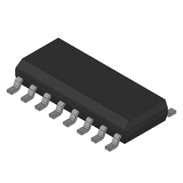
Housed in a 14-lead SOIC package (0.209" body width, 5.30 mm), the SN74LVC74ANS uses the standard 14-SO footprint. Input capacitance is 5 pF per pin, which helps maintain signal integrity on clock and data lines.