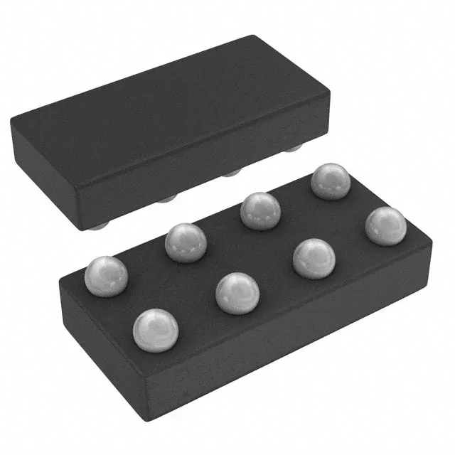
The Texas Instruments SN74LVC3G34YZPR is a triple non-inverting buffer from the 74LVC logic family, packing three independent single-bit buffer channels into an 8-bump DSBGA package that measures 1.9 × 0.9 mm.
Supply range and drive — the design decisions
That makes it a natural choice for mixed-voltage boards where a sensor output at 1.8 V needs to drive a 3.3 V logic input — the buffer's input thresholds track VCC, so the high-level input voltage scales with the supply. The 32 mA per-channel drive is enough to fan out to four or five standard CMOS loads, but not to drive a relay coil or a long cable directly. For a 50 Ω backplane trace, plan on a series resistor to limit edge rate and reflections.
DSBGA package — footprint and assembly realities
It is not a hand-solder part — the board needs a solder stencil, a reflow oven, and preferably X-ray inspection to verify bump wetting. For prototyping, the same die is also offered in a larger SOT-23 or SC-70 package under different order codes; the DSBGA is the production-optimised variant.