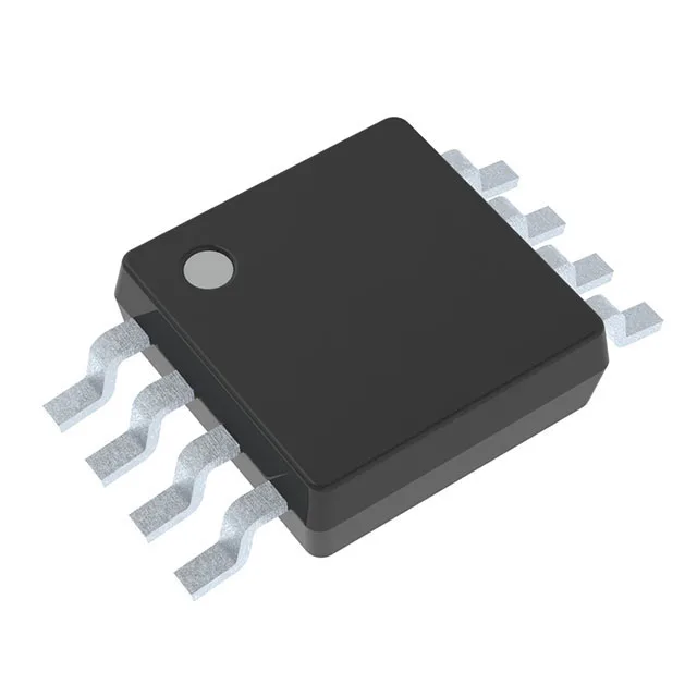
Three inverters in a 2.3 mm-wide package
The Texas Instruments SN74LVC3G04DCUR packs three independent inverter gates into an 8-VFSOP package that measures just 2.30 mm wide. Each channel provides a logic inversion with 32 mA of output drive on both the high and low side, enough to feed a half-dozen CMOS inputs or drive a short PCB trace directly.
Propagation delay and supply voltage
At 5 V and 50 pF load the propagation delay is 3.2 ns, which keeps the gate clean for clock inversion or signal fan-out up to about 80 MHz. The delay stretches at lower supply voltages — typical for the LVC family — so if your design runs at 1.8 V, budget roughly double the 5 V figure for timing closure. The input thresholds track the supply: low at 0.7 V to 0.8 V, high at 1.7 V to 2 V, making the part compatible with 1.8 V logic without extra bias.
The quiescent current maxes out at 10 µA, so it won't eat into a battery budget on a remote I/O node.
Sourcing status and compliance
The 74LVC family has broad second-source coverage across TI, Nexperia, and others, so dual-sourcing a functionally equivalent triple inverter is straightforward if your BOM calls for supply redundancy.