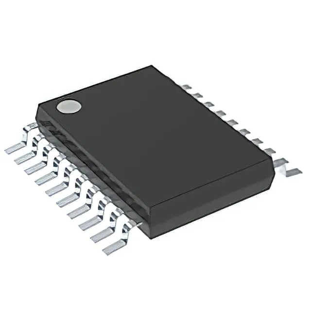
Texas Instruments SN74LVC374APW — Analog & Data Acquisition

SN74LVC374APW 74LVC D-Type Flip-Flop, 100 MHz, 20-TSSOP

MPNSN74LVC374APW
End of Life

Texas Instruments 74LVC series D-Type flip-flop, SN74LVC374APW, single 8-bit positive-edge triggered, tri-state non-inverted outputs, 100 MHz clock, 1.65V-3.6V supply, 20-TSSOP package, -40°C to 85°C.

$1.47Ref. price · indicative, final on quote
Packaging20-TSSOP (0.173", 4.40mm Width)
StockContact for availability
MOQ1 pcs
  • 100% new & originalTraceable channels only — no refurbs, no pulls, no remarked parts.
  • Date & lot codes on quoteStated per line before you commit; label photos on request.
  • MSL-compliant ESD packingMoisture-sealed bags with indicator cards; reels photo-verified.
  • PayPal buyer protectionPay by T/T, PayPal or Payoneer — card payments covered end to end.

Specifications

SN74LVC374APW Technical Specifications
ParameterValue
TypeD-Type
Series74LVC
Output typeTri-State, Non-Inverted
Trigger typePositive Edge
Mounting typeSurface Mount
Voltage1.65V ~ 3.6V
Current - quiescent10 µA
Current - output high, low24mA, 24mA
Frequency100 MHz
Operating temperature-40°C ~ 85°C (TA)
PackageTube
FunctionStandard
Case20-TSSOP (0.173\", 4.40mm Width)
Input capacitance4 pF
Number of elements1
Number of bits per element8
Max propagation delay @ v, max CL7ns @ 3.3V, 50pF

Product details

What this 8-bit D-type does in the assembly

The Texas Instruments SN74LVC374APW is an 8-bit D-type flip-flop with tri-state, non-inverted outputs, positive-edge triggered. It belongs to the 74LVC family, designed for 1.65 V to 3.6 V operation, making it a natural fit for mixed-voltage digital systems where a 3.3 V bus needs to interface with a 1.8 V core logic plane. The 20-TSSOP package is compact enough for dense boards but still hand-solderable with a fine tip and steady hands — no hot-air station required for a field swap if you have a decent iron and some flux.

100 MHz clock — timing margin for bus latching

Rated for a 100 MHz clock frequency, this part can latch address or data buses in most microcontroller and DSP systems without being the timing bottleneck. Propagation delay sits at 7 ns typical at 3.3 V with a 50 pF load, which gives you a solid setup-and-hold budget for a 10 ns to 20 ns bus cycle. If you are running a 48 MHz or 72 MHz MCU, this flip-flop will not be the one forcing wait states.

Supply range and output drive — BOM-fit details

The 1.65 V to 3.6 V supply range covers the common 1.8 V and 3.3 V rails, and the 24 mA sink/source per output can drive a handful of LED indicators or a short ribbon cable without extra line drivers. Quiescent current is only 10 µA, so it will not drain a battery-powered system in sleep mode. Input capacitance is 4 pF per pin, which keeps the bus loading light even when you have multiple flip-flops on the same address lines.

Lifecycle and sourcing reality

It is ROHS3 compliant, so it meets the latest environmental directives without a waiver. If you are filling a BOM line for a production run or a prototype batch, this is a straightforward part to qualify.

Frequently asked questions

What are direct equivalents or cross references for the SN74LVC374APW?

The 74F374SCX-NS (Fairchild 74F374) is a functional peer with a 140 MHz clock and 4.5 V supply, but it runs on 5 V only and has a narrower 0°C to 70°C temperature range. The SN74LS378N and SN74LS175NS are from the 74LS family, operate at 5 V, and offer fewer bits or different output configurations — not pin-compatible drops. For a true 3.3 V drop-in, stick with the 74LVC374 family in the same TSSOP footprint.