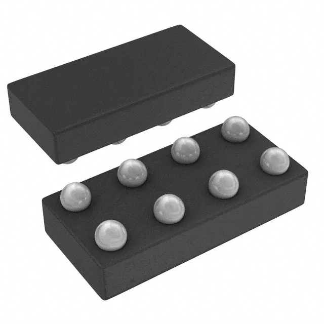
Dual XOR gate in a 1.9 mm x 0.9 mm DSBGA
The SN74LVC2G86YZPR: The device delivers 32 mA source and sink output drive and achieves a maximum propagation delay of 3.6 ns at 5 V with a 50 pF load, which keeps signal skew tight in high-speed control or data paths.
Supply range and logic-level compatibility
Input logic levels are specified as low at 0.7 V to 0.8 V and high at 1.7 V to 2 V.
Package and board-level considerations
It is ROHS3 compliant.