Texas Instruments SN74LV10ANSR — DC-DC Power Modules

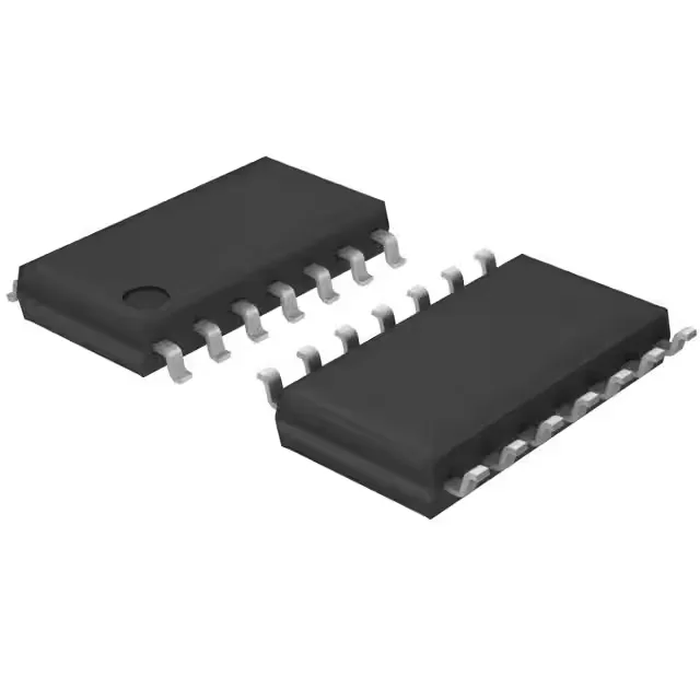
SN74LV10ANSR 74LV Triple 3-Input NAND Gate, 2V-5.5V, 14-SOIC

MPNSN74LV10ANSR
End of Life

Texas Instruments 74LV series SN74LV10ANSR, triple 3-input NAND gate, 2V to 5.5V supply, 7.9ns propagation delay at 5V/50pF, 20µA quiescent, -40°C to 85°C, 14-SOIC package, surface mount.

$0.48Ref. price · indicative, final on quote
Packaging14-SOIC (0.209", 5.30mm Width)
StockContact for availability
MOQ1 pcs
  • 100% new & originalTraceable channels only — no refurbs, no pulls, no remarked parts.
  • Date & lot codes on quoteStated per line before you commit; label photos on request.
  • MSL-compliant ESD packingMoisture-sealed bags with indicator cards; reels photo-verified.
  • PayPal buyer protectionPay by T/T, PayPal or Payoneer — card payments covered end to end.

Specifications

SN74LV10ANSR Technical Specifications
ParameterValue
Series74LV
Logic typeNAND Gate
Mounting typeSurface Mount
Voltage2V ~ 5.5V
Current - quiescent20 µA
Current - output high, low12mA, 12mA
Number of inputs3
Operating temperature-40°C ~ 85°C
PackageTape & Reel (TR); Cut Tape (CT)
Case14-SOIC (0.209\", 5.30mm Width)
Number of circuits3
Input logic level - low0.5V
Input logic level - high1.5V
Max propagation delay @ v, max CL7.9ns @ 5V, 50pF

Product details

Triple 3-input NAND gate for 2V to 5.5V logic rails

The Texas Instruments SN74LV10ANSR is a triple 3-input NAND gate from the 74LV low-voltage logic family. It integrates three independent NAND gates, each with three inputs, in a single 14-SOIC package. The part operates across a 2V to 5.5V supply range, making it a direct fit for mixed-voltage boards where a 3.3V core logic domain needs to interface with 5V-tolerant peripherals or a 2.5V I/O bank. The 74LV series is designed for low-power battery-backed or power-sensitive industrial logic, with a maximum quiescent current of 20 µA across the full temperature range.

7.9 ns propagation delay — timing budget for bus-level logic

The maximum propagation delay is 7.9 ns at 5V with a 50 pF load. This sets the timing closure floor for address decoding, control signal gating, or clock distribution where the gate sits in the critical path. At lower supply voltages the delay increases, so a 3.3V rail design should budget roughly 12-15 ns per gate for worst-case timing analysis. The 12 mA symmetric output drive at both high and low levels is enough to drive a short PCB trace or a single fan-out to another 74LV input without a buffer.

Industrial temperature grade and surface-mount footprint

Rated for -40°C to 85°C operating temperature, the SN74LV10ANSR suits outdoor telecom cabinets, factory-floor PLC I/O modules, and automotive cabin electronics that see under-hood ambient but not direct engine-bay heat. The 14-SOIC package (0.209" body width, 5.30 mm) is a standard footprint shared across the 74LV logic family, so a board layout for this gate also accepts the 74LV00 quad 2-input NAND or the 74LV08 quad 2-input AND without a respin. The supplier device package is 14-SO.

Active lifecycle and ROHS3 compliance — no LTB risk

The SN74LV10ANSR carries an active product status with ROHS3 compliance. For a production BOM this means no forced redesign cycle from obsolescence in the near term.

Frequently asked questions

What is the propagation delay of SN74LV10ANSR?

At 3.3V the delay increases; budget approximately 12-15 ns per gate for worst-case timing analysis at lower supply voltages.

Are there equivalent parts to SN74LV10ANSR?

The SN74LV11ADR is a triple 3-input AND gate in the same 74LV family and package. It is not a direct functional replacement (AND vs NAND) but shares the same supply range, propagation delay, and pin count. For a NAND function, the SN74LV00APWR is a quad 2-input NAND in a smaller package with slightly faster 7.5 ns delay.