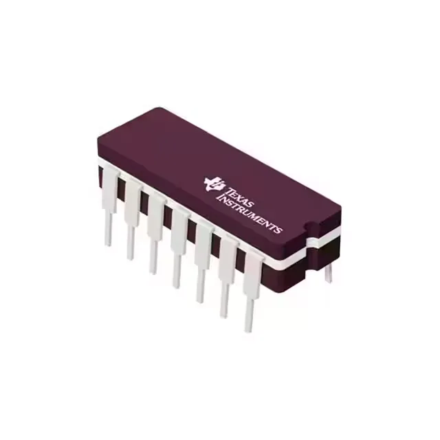
It packages four independent NOR gates in a through-hole 14-pin DIP (0.300" body), operating from a 4.75 V to 5.25 V supply over the commercial temperature range of 0°C to 70°C. The open-collector output is the defining feature: each output can sink up to 24 mA (the 'low' state) but cannot source current — it relies on an external pull-up resistor to pull the output high. This makes the part suited for wired-OR bus structures, level translation (pulling up to a different voltage than Vcc), and driving loads like relays or LEDs where the load connects between the output and a positive supply. Propagation delay is specified at 32 ns maximum into a 45 pF load at 5 V — a typical figure for the 74LS family. When budgeting timing on a backplane or shared interrupt line, that 32 ns window includes the time from any input crossing the 0.8 V (low) / 2 V (high) thresholds to the output sinking current. The quiescent supply current is 3.6 mA max for all four gates.
Open-collector output: sizing the pull-up resistor
Because the SN74LS33N output only sinks, not sources, the pull-up resistor value determines both the rise time and the high-level voltage. The 24 mA sink rating sets the minimum pull-up: at 5 V supply, a 220 Ω resistor would draw about 23 mA when the output is low — right at the limit. In practice, a 1 kΩ to 4.7 kΩ pull-up is typical for TTL-level buses, trading off speed (lower resistance = faster rise) against power (higher current when low). For a wired-OR interrupt line with several gates, the combined low-level current of all driving gates must stay under 24 mA per output. The open-collector structure allows the output high voltage to be set by the pull-up supply, which can be different from Vcc.