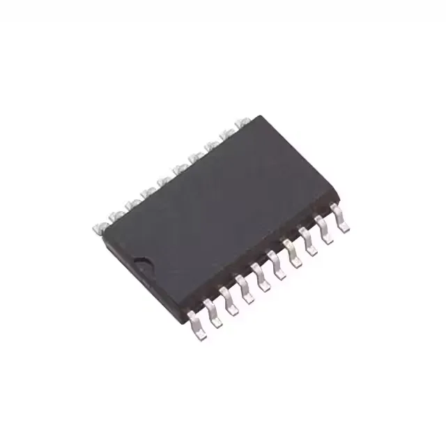
Octal D-type flip-flop for bus-oriented storage and register applications
The Texas Instruments SN74HC374DW is an octal D-type flip-flop from the 74HC family, featuring eight positive-edge-triggered flip-flops with tri-state, non-inverted outputs in a single 20-SOIC package. It operates across a 2V to 6V supply range, making it suitable for mixed 3.3V and 5V logic systems.
70 MHz clock and 15 ns propagation delay — timing budget considerations
The 70 MHz maximum clock frequency sets the upper bound for data throughput in bus-register and pipeline stages. The propagation delay of 15 ns at 6V supply with a 50 pF load is the nominal figure to use when calculating setup-and-hold margins. At lower supply voltages, expect the delay to increase — the datasheet's derating curves (not reproduced here) show the typical trade-off. For a 3.3V system at 25°C, budget roughly 20-25 ns per the family characteristics. The 3 pF input capacitance is light enough that bus loading is usually not a concern unless driving a long backplane trace.
Output drive: 7.8 mA source and sink
Each output can source or sink 7.8 mA, which is typical for the 74HC family. This drives one or two standard LSTTL loads or a handful of CMOS inputs directly. For driving LEDs, optocouplers, or relay coils, add external buffers — the 7.8 mA limit is per pin, and the package's total current ceiling (not listed here) must also be respected. The tri-state control (Output Enable, active low per the 374 function table) lets multiple devices share a common data bus without contention.
It is ROHS3 compliant. For production BOMs that require a 74HC octal flip-flop in a 20-SOIC footprint, this part is a straightforward, low-risk choice with no near-term supply discontinuity.
20-SOIC package — footprint and layout notes
The 20-SOIC body is 7.50 mm wide (0.295") with a 1.27 mm pin pitch. This is the standard SOIC-20 wide-body footprint shared by many 74HC and 74HCT logic parts. The quiescent current is just 8 µA, so self-heating is negligible even at high ambient temperatures.