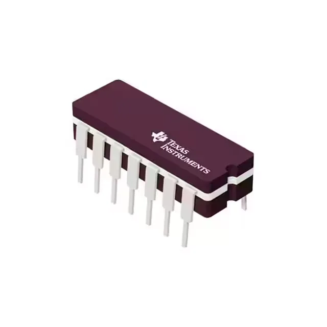
The Texas Instruments SN74F38N is a 74F-series quad 2-input NAND gate with open-collector outputs, packaged in a 14-pin through-hole DIP (0.300", 7.62mm). It contains four independent NAND gates, each with two inputs, and the open-collector output stage allows wired-OR connections, level shifting, and direct drive of loads such as LEDs, relays, or bus lines that require a pull-up to a different voltage rail. The part operates from a 4.5V to 5.5V supply and is rated for the commercial temperature range of 0°C to 70°C, making it a fit for indoor equipment, office electronics, appliance control boards, and legacy 5V logic systems where through-hole assembly is still used.
64 mA sink — the headline rating that drives the selection
The open-collector outputs are rated to sink up to 64 mA per channel, which is the key parametric for BOM fit. That sink current is what lets this gate directly drive a small relay coil, a panel LED with a series resistor, or a logic-level bus pulled up to a higher voltage. The high-level output current is listed as "-" because the output transistor is off in the high state — the pull-up resistor (external, required) determines the high-level current. The 64 mA rating is per-output; the package total dissipation still needs checking against the load duty cycle, but for typical indicator or bus applications it provides comfortable margin.
Maximum propagation delay is specified at 12.5 ns with a 5V supply and 50 pF load. This is the 74F family's speed grade — faster than the original 74LS series but not as fast as 74AC or 74AHC. For a 5V synchronous bus running at 10–20 MHz, the 12.5 ns delay leaves adequate setup-and-hold margin through one gate layer. If the design uses multiple cascaded open-collector stages with pull-up resistors, the RC time constant of the pull-up and load capacitance will dominate the total delay, so the 12.5 ns spec is the gate-only floor.
The 74F series has broad distribution support, and the DIP package continues to be manufactured for industrial and legacy-support demand.
Input logic levels and 5V compatibility
The input logic levels are standard TTL: low is 0.8V maximum, high is 2V minimum. This means the SN74F38N is directly compatible with 5V TTL and 5V CMOS logic families that output TTL-compatible levels (such as 74LS, 74S, 74F, and 5V 74HCT). It will also accept 3.3V logic outputs as long as the high-level voltage exceeds 2V — most 3.3V CMOS outputs at 3.0V or above meet this threshold. The supply range of 4.5V to 5.5V keeps it firmly in the 5V logic domain.
Package and mounting — through-hole DIP for prototyping and legacy boards
The 14-pin DIP (0.300", 7.62mm) with through-hole mounting is the traditional dual-inline package. It fits standard 0.1-inch pitch prototyping boards, wire-wrap panels, and legacy PCB layouts that were designed before surface-mount became dominant. For a repair, retrofit, or small-batch production run that uses through-hole assembly, this is the correct ordering code — the surface-mount variants (SN74F38D, SN74F38NSR) carry different suffixes.
Quiescent current and power budget
Maximum quiescent supply current is 7 mA for all four gates combined. At 5V, that is 35 mW quiescent dissipation — negligible in most designs. The dynamic power depends on the switching frequency and load capacitance, but for a typical gate used at a few megahertz, the total dissipation stays well under 100 mW. No heatsinking is needed for the DIP package in normal ambient conditions.