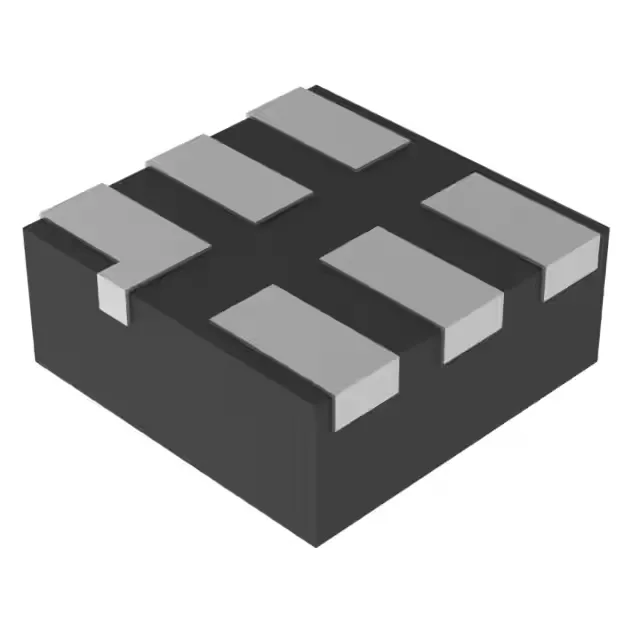
Texas Instruments SN74AUP1G32DSF2 — Analog & Data Acquisition

SN74AUP1G32DSF2 OR Gate, 0.8V–3.6V, 6.4ns @ 3.3V

MPNSN74AUP1G32DSF2
End of Life

Texas Instruments 74AUP series SN74AUP1G32DSF2 single 2-input OR gate, 0.8V–3.6V supply, 500 nA quiescent, 4 mA output drive, 6.4 ns propagation delay at 3.3V/30pF, -40°C to 85°C, 6-XFDFN package.

$0.6Ref. price · indicative, final on quote
Packaging6-XFDFN
StockContact for availability
MOQ1 pcs
  • 100% new & originalTraceable channels only — no refurbs, no pulls, no remarked parts.
  • Date & lot codes on quoteStated per line before you commit; label photos on request.
  • MSL-compliant ESD packingMoisture-sealed bags with indicator cards; reels photo-verified.
  • PayPal buyer protectionPay by T/T, PayPal or Payoneer — card payments covered end to end.

Specifications

SN74AUP1G32DSF2 Technical Specifications
ParameterValue
Series74AUP
Logic typeOR Gate
Mounting typeSurface Mount
Voltage0.8V ~ 3.6V
Current - quiescent500 nA
Current - output high, low4mA, 4mA
Number of inputs2
Operating temperature-40°C ~ 85°C
PackageTape & Reel (TR); Cut Tape (CT)
Case6-XFDFN
Number of circuits1
Input logic level - low0.7V ~ 0.9V
Input logic level - high1.6V ~ 2V
Max propagation delay @ v, max CL6.4ns @ 3.3V, 30pF

Product details

Single OR gate for the tightest power budgets

The Texas Instruments SN74AUP1G32DSF2 is a single 2-input OR gate from the 74AUP series, the industry's lowest-power logic family. It operates from 0.8V to 3.6V, making it a direct fit for battery-powered and multi-voltage designs where a standard 3.3V OR gate would draw too much idle current. The 500 nA maximum quiescent current means this gate can sit on a sensor interrupt line or a power-good combiner without draining the battery during sleep.

6.4 ns propagation delay — what it buys the bus

With a maximum propagation delay of 6.4 ns at 3.3V into a 30 pF load, this gate keeps combinatorial paths tight enough for most low-frequency control and status signals. It will not limit a 48 MHz SPI chip-select or a 1 MHz PWM enable. At lower supply voltages the delay increases, so if you are running the gate at 1.2V, budget closer to 20 ns — the datasheet curve is worth a look before signing off timing closure.

Package and footprint: 6-XFDFN (1 mm × 1 mm)

Housed in a 6-XFDFN package (supplier device package 6-SON, 1 mm × 1 mm), this part is surface-mount only.

Temperature grade and environment

Rated for -40°C to 85°C, this gate suits outdoor telecom enclosures, factory-floor I/O modules, and automotive cabin-zone logic where the ambient stays below 85°C. Not qualified to AEC-Q100, so for under-hood or extended-temperature applications, look at the AUP family's automotive-grade siblings.

Lifecycle and sourcing reality

The SN74AUP1G32DSF2 is listed as Active with ROHS3 compliance.

Frequently asked questions

What is the propagation delay for SN74AUP1G32DSF2 at 1.8V?

The evidence does not list a propagation delay at 1.8V. At 3.3V with a 30 pF load the maximum is 6.4 ns. For lower supply voltages, the datasheet provides typical curves — the delay increases as supply drops.

Does SN74AUP1G32DSF2 have internal pull-up resistors?

No. The SN74AUP1G32DSF2 is a standard CMOS OR gate with no internal pull-up or pull-down resistors on its inputs. Unused inputs must be tied to VCC or GND externally to prevent floating nodes and excess quiescent current.

What is the difference between SN74AUP1G32DSF2 and SN74LVC1G32?

The SN74AUP1G32DSF2 draws 500 nA quiescent maximum versus roughly 10 µA for the LVC version, making the AUP part the choice for battery-powered always-on circuits. The LVC variant typically offers higher output drive (24 mA vs 4 mA) and operates from 1.65V to 5.5V, so it fits 5V-tolerant legacy buses. Packages differ — the AUP comes in 6-XFDFN (1 mm × 1 mm), while the LVC is available in larger SOT-23 and SC-70 packages.