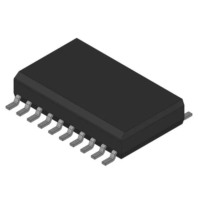
Texas Instruments SN74AS534DW — Discrete Semiconductors

SN74AS534DW D-Type Flip-Flop, 125 MHz, 20-SOIC

MPNSN74AS534DW
End of Life

Texas Instruments SN74AS534DW, D-Type flip-flop, AS series, 8-bit, positive-edge triggered, tri-state inverted outputs, 125 MHz clock, 9 ns propagation delay, 4.5-5.5 V supply, 20-SOIC, 0°C to 70°C.

$1.72Ref. price · indicative, final on quote
Packaging20-SOIC (0.295", 7.50mm Width)
StockContact for availability
MOQ1 pcs
  • 100% new & originalTraceable channels only — no refurbs, no pulls, no remarked parts.
  • Date & lot codes on quoteStated per line before you commit; label photos on request.
  • MSL-compliant ESD packingMoisture-sealed bags with indicator cards; reels photo-verified.
  • PayPal buyer protectionPay by T/T, PayPal or Payoneer — card payments covered end to end.

Specifications

SN74AS534DW Technical Specifications
ParameterValue
TypeD-Type
Output typeTri-State, Inverted
Trigger typePositive Edge
Mounting typeSurface Mount
Voltage4.5V ~ 5.5V
Current - quiescent128 mA
Current - output high, low15mA, 48mA
Frequency125 MHz
Operating temperature0°C ~ 70°C (TA)
PackageBulk
FunctionStandard
Case20-SOIC (0.295\", 7.50mm Width)
Number of elements1
Number of bits per element8
Max propagation delay @ v, max CL9ns @ 5V, 50pF

Product details

8-bit D-type register with inverted tri-state outputs

The SN74AS534DW is an 8-bit D-type flip-flop from TI's Advanced Schottky (AS) logic family. It clocks data in on the positive edge of the clock and presents the inverted state at the outputs when the output-enable is low. The tri-state outputs let multiple devices share a common bus — the inverted polarity is useful for active-low data paths or inverting buffer stages in 5 V backplane and memory-mapped I/O designs.

125 MHz clock and 9 ns propagation delay — timing headroom for synchronous buses

Rated at 125 MHz clock frequency and 9 ns max propagation delay (at 5 V, 50 pF load), this part keeps up with fast synchronous buses in 5 V systems. The 9 ns delay includes both clock-to-output and the tri-state turn-on time — a key number for setup-and-hold margin when the register feeds a synchronous FIFO or address latch. The 128 mA quiescent current is higher than later BiCMOS or CMOS logic families, so factor it into the 5 V rail budget if the board carries several bus-interface devices.

20-SOIC footprint, 0°C to 70°C commercial temperature range

Packaged in a 20-pin SOIC with 7.50 mm body width, the SN74AS534DW is a surface-mount part for commercial-temperature environments (0°C to 70°C). The supply range is 4.5 V to 5.5 V.

RoHS non-compliant — plan for exemption or alternate

The SN74AS534DW is listed as RoHS non-compliant. The lifecycle status is Active.

Frequently asked questions

Is SN74AS534DW RoHS compliant?

No, the SN74AS534DW is marked RoHS non-compliant. If your BOM requires RoHS-10 compliance, this part does not meet that requirement.

What is the difference between SN74AS534DW and SN74AS574DW?

Both are 8-bit D-type flip-flops in the same AS logic family and 20-SOIC package. The key difference is output polarity: the SN74AS534DW has inverted (inverting) tri-state outputs, while the SN74AS574DW has non-inverted outputs. Choose the 534 for active-low bus architectures or inverting buffer applications; choose the 574 for non-inverted data paths.

What is SN74AS534DW's listed type on this component line?

The listed type is D-Type, meaning it is a D-type flip-flop (data-type register) that captures the input state on the rising clock edge.