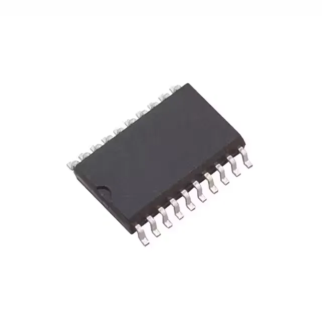
35 MHz clock — timing margin for 5V buses
The 35 MHz maximum clock frequency sets the upper data rate for this register. At 5V with a 50 pF load, the propagation delay is 16 ns max, which defines the setup-to-output window for the downstream logic.
Output drive and quiescent draw
The output stage sources 2.6 mA and sinks 24 mA per pin (high/low), which is typical for ALS logic and sufficient to drive one or two standard TTL loads or a CMOS input with a pull-up. The quiescent supply current is 19 mA — the standing draw on the 5V rail when the clock is running but outputs are static.
Active lifecycle, no obsolescence concern
For new designs or production replenishment, it is a standard catalog item with no supply-chain urgency. The 74ALS family is mature but still supported; no direct pin-compatible replacement is announced, and none is needed.