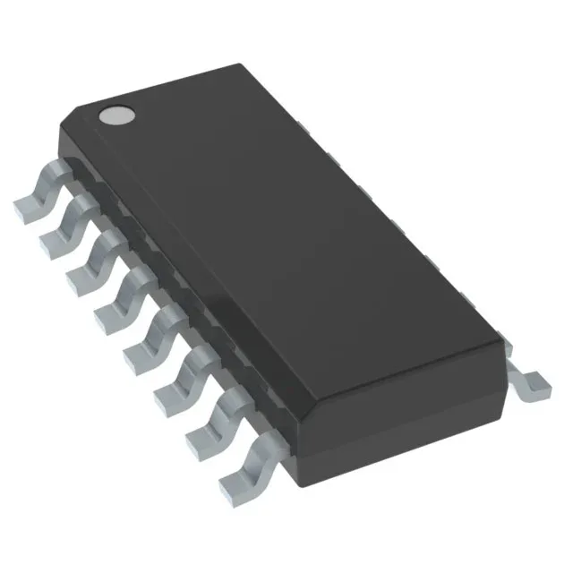
Each of the two elements stores one bit, clocked at up to 34 MHz, with a propagation delay of 18 ns into a 50 pF load at 5 V. It operates from a 4.5 V to 5.5 V supply and draws 4 mA quiescent current. The 16-SOIC footprint (0.209" body width) is a common surface-mount logic package that fits standard pick-and-place assembly.
34 MHz clock and 18 ns propagation delay — timing budget reality
The 34 MHz maximum clock frequency and 18 ns propagation delay at 5 V, 50 pF define the usable timing window. In a counter or state-machine chain, the 18 ns clock-to-output plus the next gate's setup time must fit within one clock period. At 34 MHz the period is about 29.4 ns, leaving roughly 11 ns for downstream logic and trace delay — adequate for moderate-speed bus interfaces but tight for backplane or memory-mapped I/O without pipeline registers. The positive-edge trigger is standard for most synchronous designs; the preset and reset inputs are asynchronous and active-low, so they override the clock.
5 V supply and commercial temperature — design constraints
This part is strictly a 5 V ± 0.5 V logic device. The output drive capability is 400 µA sourcing and 8 mA sinking, which is typical for ALS logic and sufficient to drive one or two standard TTL loads but not a high-fanout bus without a buffer.