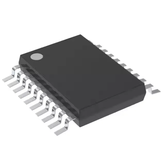
Eight-bit register with master reset — 110 MHz edge rate
Rated for 110 MHz clock frequency, this part handles high-speed data-path applications like address latching, status-register buffering, or pipeline stages in FPGA-glue logic and microcontroller expansion buses.
110 MHz clock — bus margin against slower logic
At 110 MHz, the SN74AHC273NSR provides a clock-speed advantage over the SN74LS175NS (40 MHz) and the SN74LS378N (40 MHz) from the 74LS series. Propagation delay is 11 ns at 5 V with a 50 pF load — tight enough for back-to-back registered transfers without dead cycles. The 74F174PC (80 MHz, 10 ns) comes closer in speed but lacks the wide supply range and industrial temperature rating.
Because the 74AHC family remains a standard-logic workhorse, second-source availability from other manufacturers is typical for this function.
Each output sinks or sources 8 mA (I_OH / I_OL), which is enough to drive a standard CMOS logic input, an LED indicator through a series resistor, or a low-power relay driver with external transistor gain. Quiescent current is 4 µA typical. In battery-backed or always-on sections, that draw is negligible. Input capacitance of 2.5 pF keeps the clock-line loading light, which helps maintain signal integrity on a multi-drop bus running at 110 MHz.