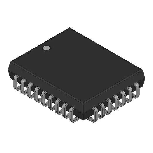
The Texas Instruments SN74ACT7200L50RJ is an asynchronous FIFO memory with a 256 x 9 organization (2.25 Kbit total). It is designed for buffering data between two clock domains or bus-width converters in 5 V logic systems. The 50 ns access time and 15 MHz data rate suit moderate-speed applications like printer buffers, industrial controller data capture, or telecom line-card packet queues. The part operates from a 4.5 V to 5.5 V supply and is specified over the commercial temperature range of 0°C to 70°C, so it is intended for indoor, non-extreme environments.
The 50 ns access time is the time from read-enable assertion to valid data on the output bus. In a typical asynchronous read cycle, the host controller must wait at least 50 ns after strobing the read line before latching data. This sets a ceiling on the system clock or cycle time: a 50 ns access time limits the read cycle to roughly 20 MHz maximum if you account for setup/hold margins. For a 15 MHz data rate (the maximum guaranteed throughput), the 50 ns access time is well within the available cycle budget, leaving margin for bus propagation delays and logic timing.
256 x 9 depth and width — buffer sizing
The 256-word depth by 9-bit width is a common size for byte-wide data plus a parity or control bit. The 9-bit width allows storage of 8-bit data with an extra bit for parity, tag, or flag. The 256-word depth provides a 256-byte buffer (plus parity), which is sufficient for short data bursts in applications like interrupt-driven UART buffering, small packet assembly, or rate-matching between a slow ADC and a fast DSP. The FIFO supports depth and width expansion (cascading multiple devices) for larger buffers.
Package and footprint: 32-PLCC (J-Lead)
The SN74ACT7200L50RJ comes in a 32-lead PLCC package (J-lead form factor), supplier device package 32-PLCC. The J-lead is a surface-mount style with leads bent under the body, requiring a PLCC socket or a reflow profile compatible with J-lead solder joints. The package is not a standard SOIC or QFP, so verify the board footprint matches the 32-PLCC land pattern. The part is marked as RoHS non-compliant, meaning it contains lead in the solder finish — check your assembly line's exemption status for leaded components.
However, it is RoHS non-compliant, which may limit its use in new designs bound for RoHS-regulated markets. If you need a lead-free alternative, the SN74ACT72241L20RJ and SN74ACT72231L20RJ are higher-speed siblings (20 ns access time) in the same 74ACT family, but verify pin-compatibility and functional equivalence before substituting.