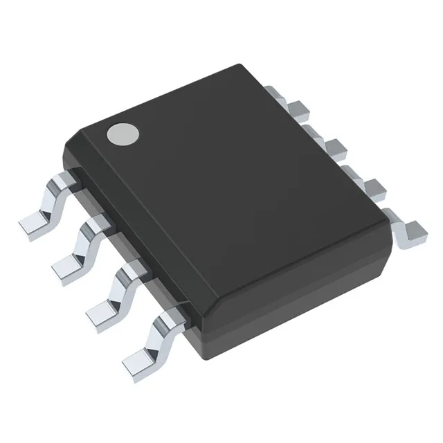
Texas Instruments SN65LVEP11DR — Clock & Timing ICs

SN65LVEP11DR 1:2 Fanout Buffer, 3.8 GHz, 8-SOIC

MPNSN65LVEP11DR
End of Life

Texas Instruments SN65LVEP11DR, Fanout Buffer (Distribution), 1:2, 3.8 GHz, ECL/PECL I/O, 2.375V–3.8V supply, 8-SOIC, -40°C to 85°C.

$5.09Ref. price · indicative, final on quote
Packaging8-SOIC (0.154", 3.90mm Width)
StockContact for availability
MOQ1 pcs
  • 100% new & originalTraceable channels only — no refurbs, no pulls, no remarked parts.
  • Date & lot codes on quoteStated per line before you commit; label photos on request.
  • MSL-compliant ESD packingMoisture-sealed bags with indicator cards; reels photo-verified.
  • PayPal buyer protectionPay by T/T, PayPal or Payoneer — card payments covered end to end.

Specifications

SN65LVEP11DR Technical Specifications
ParameterValue
TypeFanout Buffer (Distribution)
Mounting typeSurface Mount
Voltage2.375V ~ 3.8V
Frequency3.8 GHz
Operating temperature-40°C ~ 85°C
InputECL, PECL
OutputECL, PECL
PackageTape & Reel (TR); Cut Tape (CT)
Case8-SOIC (0.154\", 3.90mm Width)
Number of circuits1
Ratio - Input:Output1:2
Differential - Input:OutputYes/Yes

Product details

3.8 GHz fanout buffer for differential clock distribution

The Texas Instruments SN65LVEP11DR is a 1:2 fanout buffer designed for high-speed differential clock and data distribution. It accepts ECL or PECL inputs and delivers two matched ECL/PECL outputs, maintaining signal integrity up to 3.8 GHz. The part operates from a 2.375 V to 3.8 V supply, covering common 2.5 V and 3.3 V logic rails, and is specified across the industrial temperature range of -40°C to 85°C. Typical applications include clock fan-out in telecom switches, data center switches, test equipment, and any serial link requiring low-skew distribution of a high-frequency reference.

Supply range and differential I/O — what they mean for your design

The 2.375 V to 3.8 V supply range lets this buffer run directly from a 2.5 V or 3.3 V rail without an external regulator, simplifying power-tree design. Because both input and output are differential ECL/PECL, the part mates directly to common high-speed clock sources (e.g., LVDS oscillators with AC coupling, or PECL VCXOs) and to downstream ECL/PECL loads such as SerDes reference inputs or FPGA clock pins. The differential path also gives common-mode noise rejection, important when the buffer sits near switching regulators or on a noisy backplane.

Package and footprint

Housed in an 8-pin SOIC package (8-SOIC, 0.154" body width, 3.90 mm), the SN65LVEP11DR uses a standard surface-mount footprint compatible with automated assembly. No exposed pad or thermal via is required at the rated dissipation levels. The -40°C to 85°C operating range covers most industrial and telecom environments.

Lifecycle and sourcing

It is ROHS3 compliant. For dual-sourcing or higher fan-out requirements, the CDCLVP1204RGTR offers a 2:4 LVPECL fanout buffer in a similar supply range, though it uses a different package (QFN) and is not a pin-for-pin drop-in. Sourcing is confirmed through independent distribution; availability and current pricing are quoted against an RFQ.

Frequently asked questions

Does SN65LVEP11DR support differential inputs and outputs?

Yes, both the input and output are differential, and the part accepts ECL or PECL levels on the input side while delivering ECL/PECL outputs.

Is SN65LVEP11DR compatible with LVPECL?

The part uses ECL/PECL I/O levels. LVPECL is a 3.3 V variant of PECL; with a 3.3 V supply the SN65LVEP11DR operates within LVPECL voltage swings and is compatible with LVPECL signals.