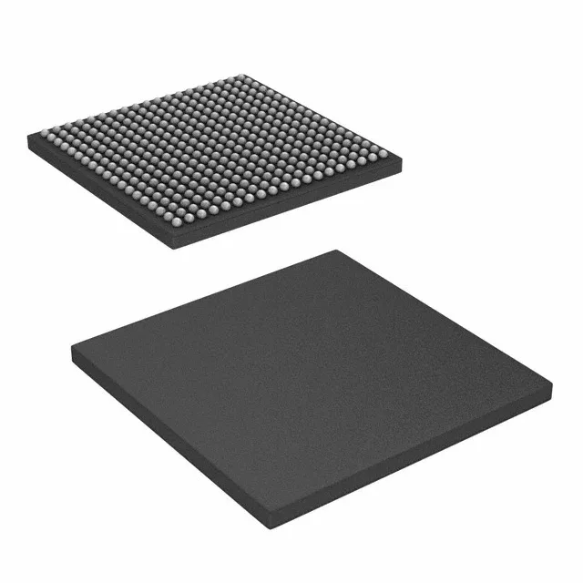
Texas Instruments OMAPL138EZWTA3R — DC-DC Power Modules

TI OMAPL138EZWTA3R ARM9 + C674x DSP, 375 MHz, 361-NFBGA

MPNOMAPL138EZWTA3R
End of Life

Texas Instruments OMAP-L1x series, OMAPL138EZWTA3R, ARM926EJ-S + C674x DSP, 375 MHz, dual USB (1.1 + PHY, 2.0 + PHY), SATA 3Gbps, 10/100 Ethernet, 361-NFBGA, -40 to 105°C.

$28.32Ref. price · indicative, final on quote
Packaging361-LFBGA
RoHSROHS3 Compliant
SeriesOMAP-L1x
Independent supplier — new & surplus stockAuthenticity-screened · ESD-safe packingListing updated Aug 2026

Specifications

OMAPL138EZWTA3R specifications
ParameterValue
SeriesOMAP-L1x
MountingSurface Mount
Voltage - i (O)1.8V, 3.3V
Additional interfacesHPI, I²C, McASP, McBSP, MMC/SD, SPI, UART
Display & interface controllersLCD
Operating temperature-40°C ~ 105°C (TJ)
Number of cores (Bus width)1 Core, 32-Bit
USBUSB 1.1 + PHY (1), USB 2.0 + PHY (1)
SATASATA 3Gbps (1)
Speed375MHz
PackageTape & Reel (TR); Cut Tape (CT)
Ethernet10/100Mbps (1)
Core processorARM926EJ-S
Case361-LFBGA
RAM controllersSDRAM
Co-Processors (DSP)Signal Processing; C674x, System Control; CP15
Security featuresBoot Security, Cryptography
Graphics accelerationNo

Product details

ARM926 + C674x DSP — what this dual-core processor brings to the BOM

The Texas Instruments OMAPL138EZWTA3R is a dual-core applications processor combining an ARM926EJ-S general-purpose core with a C674x floating-point DSP on a single die. The ARM core handles OS and control tasks at 375 MHz while the DSP offloads real-time signal processing — audio, vibration analysis, motor control loops — without an external DSP chip. This architecture collapses what used to be a two-chip BOM into one 361-NFBGA package, saving board area and reducing interconnect complexity. The peripheral set is built for industrial gateway and data-acquisition roles: dual USB ports (one USB 1.1 with PHY, one USB 2.0 with PHY), a SATA 3Gbps interface for local storage, and a 10/100 Ethernet MAC for network connectivity. Additional interfaces including HPI, I²C, McASP, McBSP, MMC/SD, SPI, and UART cover sensor fusion, display (LCD controller), and legacy serial links. The SDRAM controller keeps memory cost predictable — no DDR3 layout complexity required. The 1.8V and 3.3V I/O rails let it interface directly with common sensor and memory voltage domains without level shifters on every line.

Security and boot — factory-programmed or field-locked

On-chip security features include boot authentication and cryptography acceleration, allowing encrypted firmware images and secure boot chain validation.

For a production BOM freeze, this means the part is still in TI's standard ordering system and factory pipeline — not a surplus-channel scavenge. The ROHS3 compliance covers current environmental regulations across EU and Asia markets without exemption paperwork.

Frequently asked questions

What are the alternatives or cross references for OMAPL138EZWTA3R?

The closest sibling within the OMAP-L1x family is the OMAPL138BZWTA3R. The difference is in the silicon revision — the -EZW- variant carries an extended feature set versus the -BZW- stepping. Both share the same ARM926EJ-S + C674x DSP architecture, 375 MHz speed, 361-NFBGA package, and pinout. For a drop-in replacement, verify the silicon revision requirements with your firmware team before swapping.

What is OMAPL138EZWTA3R's listed USB and SATA configuration?

The part integrates two USB ports: one USB 1.1 with integrated PHY and one USB 2.0 with integrated PHY. For mass storage, it includes a single SATA 3Gbps port. These are on-chip — no external PHY chips needed for the USB interfaces, which saves BOM cost and board area.

What voltage rails does OMAPL138EZWTA3R require?

The I/O voltage is rated for 1.8V and 3.3V domains. The core voltage is not specified in this listing; refer to the TI datasheet for the VDD and PLL supply values. The 1.8V/3.3V I/O rails allow direct connection to common SDRAM, NOR Flash, and sensor interfaces without external level translators.