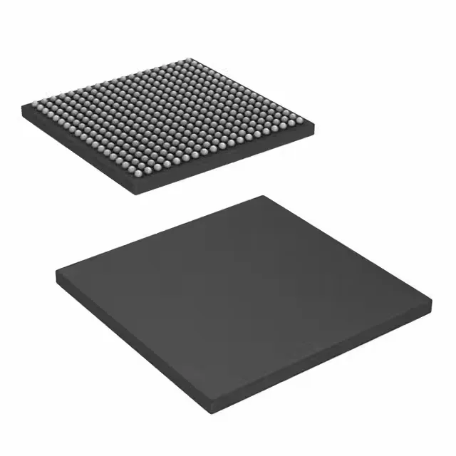
The Texas Instruments OMAPL138EZWTA3 is a heterogeneous dual-core processor pairing an ARM926EJ-S general-purpose core with a C674x floating-point DSP, clocked at 375 MHz. This architecture lets a single chip handle both control-plane tasks and real-time signal processing — motor control loops, audio encoding, vibration analysis, or protocol bridging — without a separate DSP or FPGA. On-chip peripherals include USB 1.1 and USB 2.0 each with integrated PHY, a SATA 3 Gbps port, and a 10/100 Mbps Ethernet MAC, so the part can serve as a system hub in industrial gateways, human-machine interfaces, or data-acquisition nodes. The LCD controller drives a local display directly, and the memory interface supports SDRAM, keeping BOM cost predictable.
The 361-NFBGA package (16x16 mm) requires controlled reflow and X-ray inspection — standard for a BGA of this density, but worth factoring into assembly yield planning if your line is used to QFPs.
Supply voltage and I/O flexibility
The I/O voltage is configurable at 1.8 V or 3.3 V, which means the OMAPL138EZWTA3 can interface directly with legacy 3.3 V peripherals (serial Flash, UART transceivers, sensors) or switch to 1.8 V for lower-power memory interfaces. The core voltage is derived from an internal regulator; the board design needs the appropriate supply rails for each I/O bank. Additional interfaces include HPI, I²C, McASP, McBSP, MMC/SD, SPI, and UART, covering most industrial communication buses without external level shifters.
Security and boot options
Boot security and cryptography features are built in, allowing encrypted firmware storage and authenticated boot — relevant if the end product needs to resist cloning or tampering in field-deployed equipment. The system-control coprocessor handles memory management and cache coherency between the ARM and DSP cores.
That means no last-time-buy scramble and no forced redesign for a replacement.