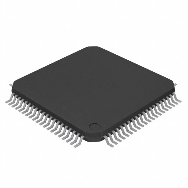
96 KB FRAM — what it changes in firmware strategy
Its program memory is 96 KB of FRAM, not flash — meaning near-instant write cycles, single-cycle endurance rated orders of magnitude beyond flash, and no erase-before-write penalty. For a firmware engineer, this eliminates the OTA staging-area sizing problem: you can treat FRAM like a unified memory for code and data, and wear-leveling becomes optional rather than mandatory. The 16 MHz CPU speed is adequate for sensor fusion loops, low-speed control, and communication protocol handling, but not for high-rate DSP or video.
63 I/O and the peripheral mix — what fits on the bus
The I²C and SPI interfaces share the same module in some MSP430 families, but here they are independent — you can run I²C and SPI simultaneously without bit-banging.
Industrial temperature grade — deployment scope
For timing-sensitive protocols like CAN or high-precision RTC, an external crystal or resonator is still the safer call.
Lifecycle status — active, no LTB pressure
For a second-source or pin-compatible alternate within the MSP430 FRAM family, the MSP430FR6888 (base product number) shares the same 80-LQFP footprint and peripheral set across density variants — but verify the exact memory and feature set against your firmware image size.