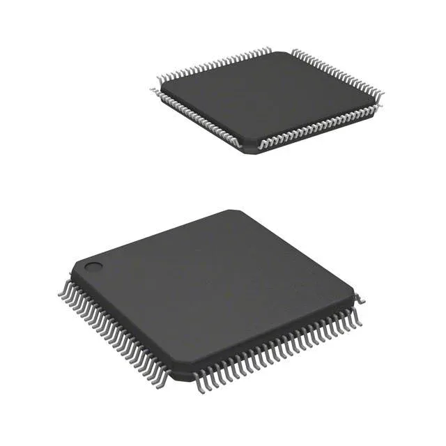
FRAM-based MCU for data-logging and low-power control
The device integrates a 16x12-bit ADC, a segment LCD controller, DMA, brown-out reset, and PWM timers, with connectivity covering I²C, SPI, UART, and IrDA.
64 KB FRAM — no erase cycles, no wear-leveling overhead
FRAM writes at the byte level with a 100 trillion cycle endurance typical for the MSP430 FRAM family. For a design that stores configuration parameters or sensor logs every few seconds, this eliminates the Flash sector-erase latency and the software wear-leveling logic otherwise required. The 2K x 8 RAM handles stack and scratchpad data; the FRAM holds both code and non-volatile data in a single unified memory map.
83 I/O and 16x12-bit ADC in a 100-LQFP
The 100-LQFP (14x14 mm) package brings out 83 general-purpose I/O pins, enough to interface with a parallel LCD, keypad matrix, and multiple external sensors without an I/O expander. The 16-channel 12-bit ADC samples at up to 200 ksps typical — sufficient for multi-channel analog front ends in flow or pressure sensing.
For BOM planning, this means standard lead times through distribution and no forced redesign horizon.