256 KB FRAM — the real story for your BOM
Its headline feature is 256 KB of FRAM program memory — a non-volatile storage that writes at bus speed, consumes negligible power, and endures 10^15 write cycles. That means no wear-leveling code, no erase-before-write delays, and the ability to treat program memory like data RAM for over-the-air updates or data logging. The 8K x 8 RAM handles stack and scratchpad. For a design that wakes, samples, logs, and sleeps, this FRAM architecture cuts firmware complexity and extends battery life compared to a Flash-based MCU with similar peripheral count.
68 I/O and 20-channel 12-bit ADC — peripheral fit for sensor fusion
The connectivity set includes I²C, IrDA, SPI, and UART/USART, so it talks to common digital sensors and radios without external level shifters.
6×6 mm BGA — plan the assembly process now
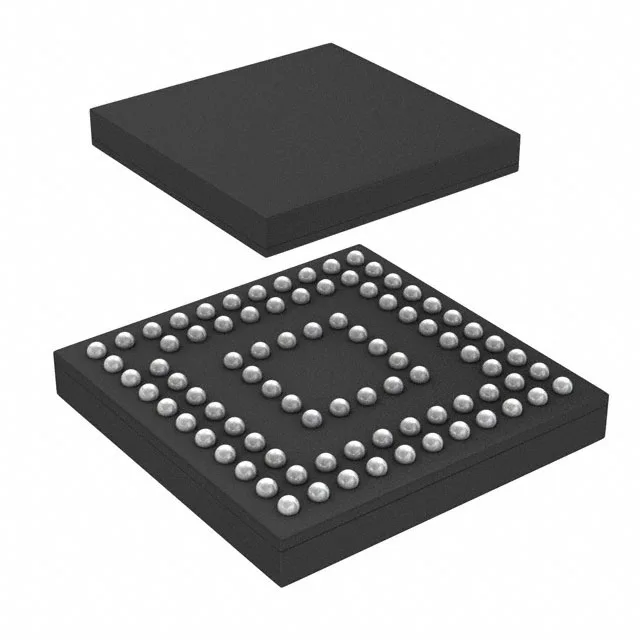
The MSP430FR59941IZVW comes in an 87-VFBGA package (supplier device package 87-NFBGA, 6x6 mm). That is a fine-pitch BGA — not a hand-solderable part without a stencil and a reflow oven or hot-air station. If your prototype or low-volume run needs hand assembly, consider the LQFP-100 variant in the same MSP430FR5994 family (different pin count, not drop-in). For production, plan for X-ray inspection and a controlled reflow profile.