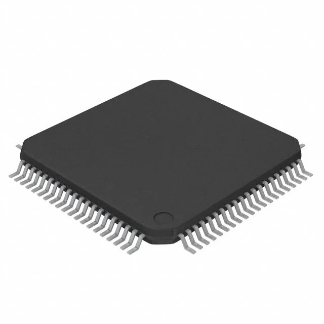
FRAM memory — the real differentiator here
What sets it apart from the usual Flash-based MCU is the program memory: 128 KB of FRAM (ferroelectric RAM). FRAM writes at near-SRAM speed, consumes far less active power per write than Flash, and tolerates 10^15 write cycles — no erase-before-write penalty, no wear-leveling firmware needed. Combined with 8 KB of conventional SRAM, this memory architecture suits data-logging, over-the-air firmware updates, and any application where the MCU wakes, writes a record, and goes back to sleep without waiting on a Flash page erase.
Supply range and battery-fit
That matters for the bill of materials count and for quiescent current in always-on sense nodes.
Peripheral set for sensor fusion and control
The built-in brown-out detect, POR, DMA, and PWM peripherals reduce external supervisor ICs and simplify the power-up sequencing. Both an external crystal and the internal oscillator are supported, so a low-cost RC-based clock is feasible for non-timing-critical code.
That means no supply-chain clock ticking for new designs or long-life BOMs.