128 KB FRAM — no wear-leveling tax, no erase-before-write
Its program memory is 128 KB of FRAM, not Flash — meaning single-cycle writes at the bus speed, no erase cycles, and a rated endurance that effectively never wears out in normal embedded use. The 8 KB of SRAM handles stack and scratchpad, while the 68 GPIOs give plenty of headroom for sensor arrays or parallel displays. This is the part you pick when you want unified memory — FRAM for both code and data logging — without the 10 kB/s write bottleneck of EEPROM.
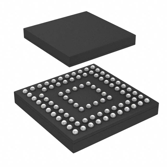
The 87-NFBGA package, 6x6 mm, packs the die and 68 I/O into a 0.5 mm pitch ball array.
16 MHz core — what the speed rating actually governs
16 MHz is the CPUXV2 clock ceiling. At that frequency, the FRAM controller inserts zero wait states for most accesses, so the core runs at full throughput — no flash wait penalty like on older MSP430s. The 12-bit ADC samples at up to 200 ksps, and the DMA can move data without CPU intervention. If your control loop needs a 10 kHz sensor read with a PID update every 100 µs, this is enough headroom. The brown-out reset and POR peripherals keep the MCU from corrupting FRAM during a power glitch, which is the main failure mode to guard against in battery-backed designs.