128 KB FRAM — unified code and data, no erase penalty
Its headline feature is 128 KB of FRAM program memory — a non-volatile storage that combines the read speed of SRAM with the non-volatility of Flash, but without the write-cycle overhead or sector-erase latency of Flash or EEPROM. This makes it a strong fit for applications that log data frequently, update firmware over the air, or need to retain state through power loss without a backup battery.
16 MHz core — enough for sensor fusion and control loops
The CPUXV2 core runs at 16 MHz, which is modest by modern MCU standards but entirely adequate for the low-power, real-time control tasks this part targets — reading a 17-channel 12-bit ADC, running a PID loop, or managing a UART/I²C sensor network. The clock tree supports both external and internal oscillators, so a design can trim the BOM by omitting the external crystal when the internal RC meets the timing budget.
The supply range of 1.8V to 3.6V lets it run directly from a 3.6V Li-ion cell or a 3.3V regulated rail, and the 1.8V floor supports battery operation down to near-depletion without a boost converter.
54 I/O in a 64-LQFP — practical footprint for mixed-signal boards
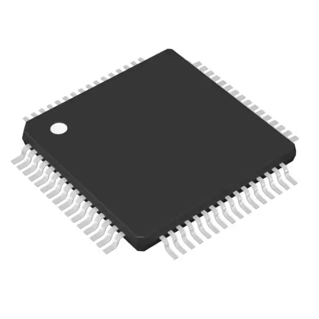
The 64-LQFP package (10x10 mm body) brings out 54 general-purpose I/O pins alongside the 17-channel 12-bit ADC, brown-out detect, POR, PWM, and watchdog peripherals. The LQFP footprint is hand-solderable and rework-friendly — no BGA reflow or X-ray inspection needed.
There is no last-time-buy or NRND notice on this base product number. For dual-sourcing resilience, the MSP430FR59xx family includes several density and package variants that share the same core and peripheral set, though pin compatibility should be verified against the specific target variant.