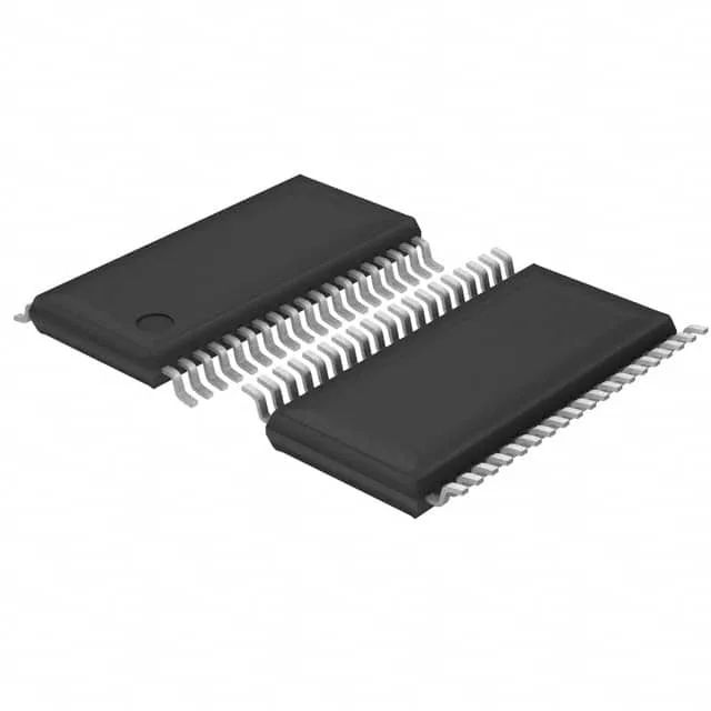
FRAM memory — the real differentiator in this MSP430
For a firmware engineer, that means you can treat the code space as a unified memory pool: store calibration constants, data logs, or OTA staging buffers right alongside the executable image without wear-leveling or sector-erase delays.
16 MHz CPU — enough for the control loop, not for heavy DSP
The 16 MHz clock ceiling is typical for the MSP430 FRAM series — it delivers about 16 MIPS, which is comfortable for sensor polling, PID loops, communication protocol handling, and real-time event response. It will not run floating-point audio processing or video; the part is sized for the battery-powered edge node that wakes, reads a sensor, logs a result, and goes back to sleep. The internal oscillator means no external crystal is required for many applications, saving two pins and a few cents on the BOM.
Peripherals and I/O — what you get on 31 pins
The DMA engine offloads data transfers between ADC and FRAM without CPU intervention, which keeps the core asleep longer. The 1 K x 8 RAM is small — it is meant for stack and temporary variables, not large buffers; persistent data lives in FRAM.