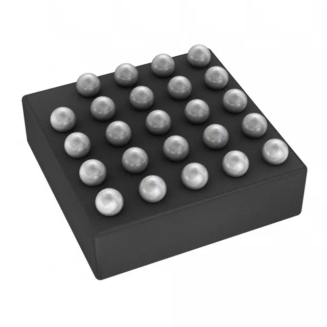
What this MSP430FR5738IYQDR brings to a low-power design
Its program memory is 16 KB of FRAM — ferroelectric RAM that combines the non-volatility of Flash with the write speed and endurance of SRAM. That means you can treat it almost like a unified memory: store code, log data, and update firmware in the field without worrying about write-cycle limits or erase-before-write delays.
FRAM: why it changes the memory trade-off
FRAM writes at bus speed — no page program or erase cycles. For a battery-powered sensor node that logs data and occasionally updates its firmware over the air, this eliminates the power penalty of Flash writes and the wear-leveling complexity. The 16 KB FRAM holds both code and data; you can partition it as needed. The 1 KB SRAM covers runtime variables and DMA buffers.
24-DSBGA package — plan the rework flow
This comes in a 24-ball DSBGA (diameter 0.4 mm balls on a 0.5 mm pitch). That's a tiny footprint — about 2.5 mm per side. Hand rework is possible with a hot-air station and a fine-tip stencil, but the small ball size means the board's solder-mask registration and pad finish matter. The part is surface mount only, and the package has no exposed thermal pad; all dissipation goes through the balls and the board copper.
For a new design, this is a clean choice — no supply-chain clock ticking.