That eliminates the write-buffer and wear-leveling logic a Flash MCU would need for frequent data logging or parameter updates. The 2K x 8 RAM is modest but sufficient for sensor buffering and protocol stacks in this class.
Package reality — 24-DSBGA
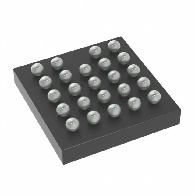
The MSP430FR2632IYQWR comes in a 24-DSBGA package (also listed as 24-UFBGA). This is a very small BGA — roughly 2.4 mm × 2.4 mm — with 17 usable I/O. The footprint requires a multi-layer PCB with micro-vias or via-in-pad for fanout; it is not a hand-solderable part. Plan for a stencil design with 0.3 mm or smaller solder-mask-defined pads. The 24-DSBGA is the only package option for this specific order code, so board area is the trade-off against ease of assembly. Surface-mount only, consistent with the DSBGA land pattern. No exposed thermal pad — junction-to-ambient thermal performance depends on PCB copper area and via count under the BGA.
For a BOM line, this means no imminent requalification risk — you can commit to this part for a production run without planning a migration.
Sourcing posture
This is a current-production TI part, available through the independent distribution channel. No allocation or long-lead flags are typical for this series as of the current quarter. If you are filling a BOM line, this is a straight-forward source — no broker scavenger hunt, no date-code lottery.