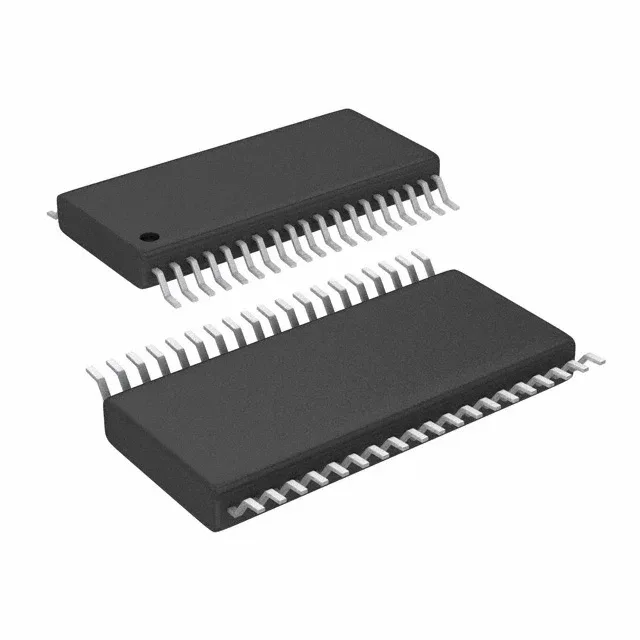
What this 16-bit FRAM MCU brings to a BOM
It belongs to the MSP430 FRAM family, where the program memory is 16 KB of FRAM — a non-volatile memory that writes at near-SRAM speed and supports over 10^15 write cycles, unlike Flash. The device integrates 2 KB of SRAM, a 10-channel 12-bit ADC, a 4-channel 12-bit DAC, and serial interfaces including I²C, SPI, and UART.
24 MHz core and FRAM — what they mean for firmware and throughput
The 24 MHz clock rate is the CPU's maximum operating frequency. For a 16-bit RISC core, this delivers enough throughput for real-time control loops like PID in motor drives or periodic sensor reads without needing an external timer. The FRAM program memory eliminates the write-erase cycle overhead of Flash — firmware updates over UART or I²C can write new code in-place without sector-erase delays. The 2 KB SRAM is modest; data logging and large buffers will need external memory or careful allocation.
Integrated ADC and DAC — analog front-end without extra chips
The 10-channel 12-bit ADC and 4-channel 12-bit DAC on-chip reduce external component count in mixed-signal designs. The ADC can sample multiple analog inputs (e.g., temperature, pressure, current sense) sequentially, while the DAC can generate analog setpoints or bias voltages. This integration saves board area and BOM cost in applications like programmable power supplies or sensor conditioners.
38-TSSOP package — rework and layout notes
The 38-TSSOP (0.173" body width, 4.40 mm) is a fine-pitch surface-mount package. It reworks well under hot air with a fine nozzle — the leads are exposed, so inspection and touch-up are straightforward. The pad layout should match the supplier package drawing; the 0.65 mm pitch demands a stencil with good aperture alignment for consistent solder paste volume.