What the FRAM means for your design
That changes how you handle data logging, calibration constants, and firmware updates: you can write to it on every control loop iteration without wearing it out, and the data survives a power loss without a backup battery. The 4K x 8 SRAM is modest — enough for a modest control stack and a few sensor buffers, but you will want to keep your main data structures in FRAM and use the SRAM for scratchpad and stack. The 24 MHz clock is the ceiling; at that speed the CPU16 core executes most instructions in one or two cycles, so it handles real-time control loops and communication protocol handling without breaking a sweat.
Peripherals and connectivity for sensor fusion
This part packs an 8-channel, 12-bit SAR ADC — enough resolution for reading thermocouples, strain gauges, or current-sense resistors with decent accuracy. The I²C, SPI, and UART interfaces let it talk to external sensors, displays, or a host processor. IrDA support is a bonus for wireless optical links in medical or industrial handhelds. Built-in brown-out reset and power-on reset mean you can skip the external supervisor IC in many designs. The PWM module drives small motors, LEDs, or solenoid valves directly. The watchdog timer keeps the system alive in unattended installations.
Package, power, and temperature — the BOM-fit details
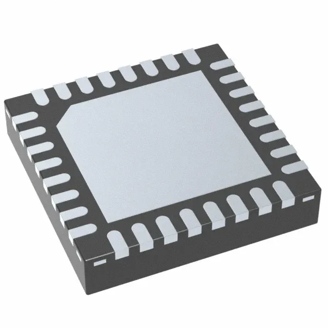
Housed in a 32-VFQFN with exposed pad (4x4 mm body), this is a compact surface-mount package suited for space-constrained PCBs.
For dual-sourcing resilience, the MSP430FR2155 family includes several density and package variants that share the same CPU16 core and peripheral set, though pin compatibility varies with the package option.