The 20 MHz clock rate is the nominal CPU speed — the core can run code directly from Flash at that frequency, but the flash wait state controller needs to be configured correctly during clock tree setup. The CPUXV2 is a 16-bit RISC architecture with a hardware multiplier, and the 512 KB Flash gives room for a full protocol stack (USB, LCD driver, sensor fusion) plus a bootloader for field updates. The 66 KB of RAM supports multi-packet USB buffers, large ADC result arrays, or a real-time operating system heap without external memory. The integrated DMA controller can move data between peripherals and RAM without CPU intervention, which is useful for streaming ADC samples or servicing USB endpoints at full speed.
USB, LCD, and analog integration — peripheral set for mixed-signal control
This MCU includes a full-speed USB 2.0 interface (device/host/OTG) with an integrated PHY, so no external USB transceiver is needed. An integrated LCD driver (segment type) can directly drive a glass LCD panel without an external controller — useful for metering, medical displays, or control panels.
113-ball BGA — layout considerations for the 7x7 mm package
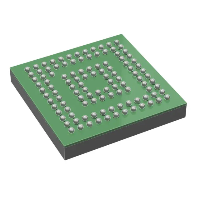
The MSP430F6659IZCAT comes in a 113-VFBGA package (also specified as 113-NFBGA, 7x7 mm body). With 74 general-purpose I/O pins, the package provides ample GPIO for parallel interfaces or keypad scanning.