20 MHz MSP430 CPUXV2 with USB 2.0 — what it buys you
This is the part you pick when you need USB connectivity in a battery-powered or industrial sensor node without adding a second chip.
256 KB Flash / 18 KB RAM — firmware headroom
That is enough space for a USB composite device (HID + CDC) with a modest control loop, a data-logging buffer, and a bootloader. The RAM is tight if you plan to double-buffer USB packets and run a large display buffer — budget carefully. The Flash endurance is rated for 100k write/erase cycles per sector, typical for MSP430, so wear-leveling is not critical unless you are logging configuration changes every few seconds.
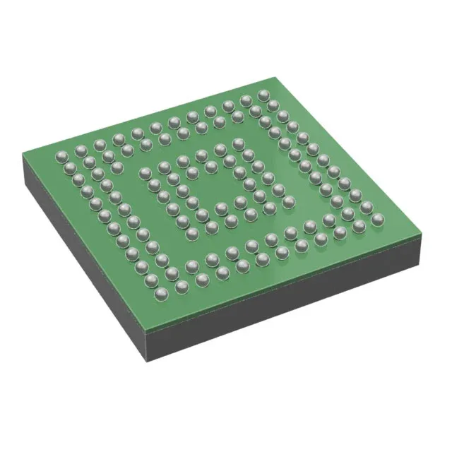
113-NFBGA (7x7 mm) — layout and reflow
That is a fine-pitch BGA — you need a solder stencil, a reflow oven, and X-ray inspection to verify joints. No field-swapping this one with a soldering iron; plan for a rework station if you are supporting field returns. The 74 I/O count gives plenty of GPIO for a keypad, display, and sensor interface, but every signal is on a BGA ball — route the breakout fan-out carefully in the first two layers.