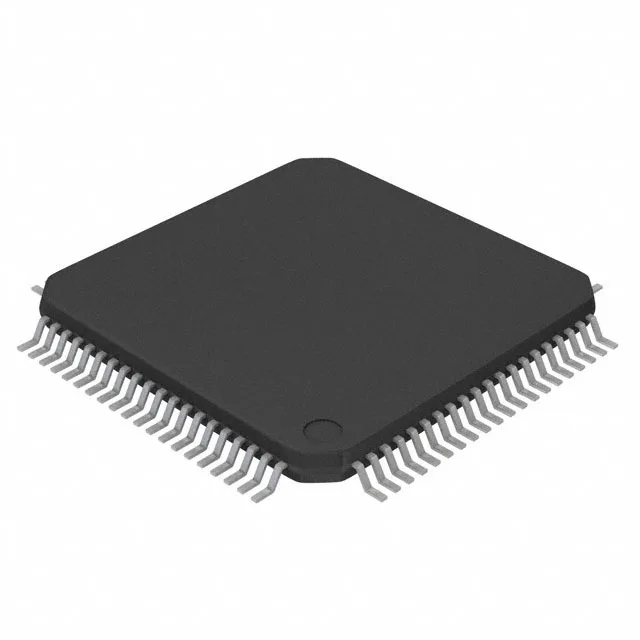
16-bit MCU with USB for low-power edge nodes
The 80-LQFP package exposes 63 I/O lines and integrates a 12-bit ADC with 16 channels, an internal oscillator, and peripherals including DMA, PWM, brown-out reset, and a watchdog timer. Typical applications span USB-based data loggers, sensor gateways, portable medical devices, and industrial control panels where the USB interface offloads host communication without an external bridge chip.
25 MHz clock and wake-up energy budget
The 25 MHz CPU clock is the top end for this MSP430F5xx part. In a battery-powered LoRa or Zigbee sensor node, running the core at full speed during brief active windows and then dropping into a low-power sleep mode is the standard strategy. The 6K x 8 RAM limits packet buffers — a USB CDC-ACM virtual COM port with a 512-byte buffer plus a 1 KB sensor data queue leaves about 4.5 KB for stack and variables, which is tight for a full TCP/IP stack but comfortable for a custom serial protocol or a lightweight CoAP endpoint.
No exposed thermal pad — the package dissipates through the leads, so keep the ambient below 85°C if the I/O load is high.
For dual-sourcing resilience, the MSP430F5529 (with 128 KB Flash and 10K x 8 RAM) is a drop-in software-compatible upgrade in the same package, though the extra memory and slightly different peripheral set require a firmware recompile.