25 MHz CPUXV2 core — throughput for control loops
The 16-bit architecture keeps code density tight, which matters when the 128 KB Flash budget has to hold both application firmware and a bootloader.
The Flash is sufficient for moderately complex firmware stacks — think a Modbus RTU slave with PID loops, or a data-logger with a FAT filesystem. The 16 KB RAM handles a few hundred bytes of stack plus several 1 KB DMA buffers for ADC or serial data without overflow.
Peripheral set — connectivity and analog
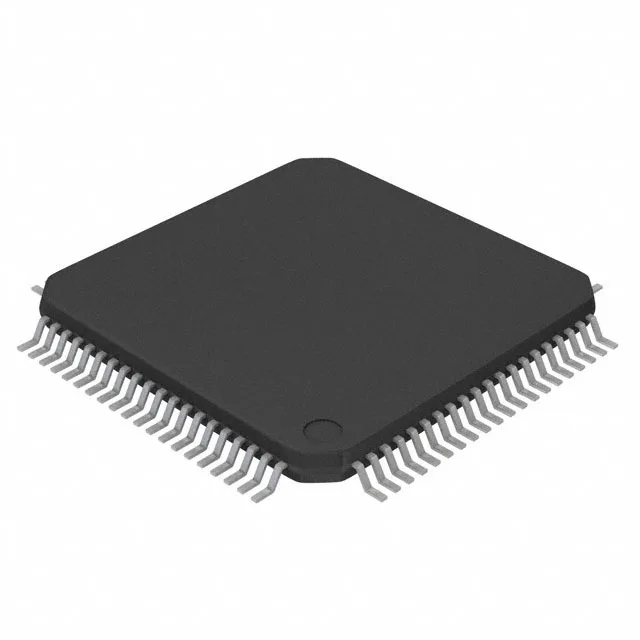
Package and footprint — 80-LQFP (12x12 mm)
Housed in an 80-pin LQFP with a 12x12 mm body, the MSP430F5418AIPNR uses a 0.5 mm pitch. The supplier device package is 80-LQFP (12x12).