At 20 MHz the CPUXV2 pipeline keeps single-cycle access to the register file and most instructions complete in one or two clocks. That is enough headroom for a 100 kHz control loop with a PID update and a UART transaction between samples. If your application needs to toggle a GPIO at a precise rate or service a timer interrupt with low jitter, the 20 MHz clock gives you a 50 ns tick — fine-grained enough for most sensor polling and PWM generation tasks.
512 KB Flash and 66K x 8 RAM — sizing the firmware image
The 512 KB Flash is large enough to hold a full protocol stack (say, a Modbus RTU library plus a bootloader) with room left for field-upgradeable application code. The 66K x 8 RAM supports multiple data buffers and a modest RTOS heap without tight packing. If you are porting code from a smaller MSP430, the extra RAM means you can keep a larger look-up table or a frame buffer in SRAM instead of paging from Flash.
Peripherals and connectivity — what is on the die
Package and supply — board-level fit
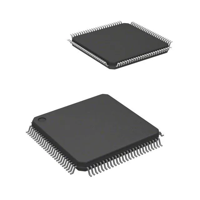
The MSP430F5359IPZ comes in a 100-pin LQFP (14x14 mm body, 0.5 mm pitch) — a common footprint that routes easily on a two-layer board.
Sourcing and lifecycle — what the BOM engineer needs
For dual-sourcing resilience, the MSP430F5xx family includes pin-compatible density variants (e.g., 256 KB Flash options) that share the same 100-LQFP footprint and peripheral map — a straightforward fallback if the 512 KB version is on allocation.