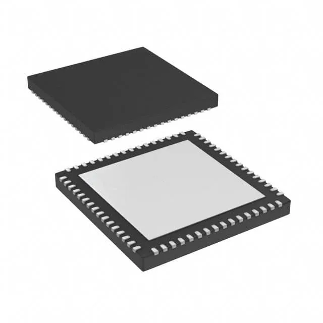
Dual DPLL clock synchronizer for precision timing
It accepts four differential or single-ended inputs (CML, HCSL, LVDS, LVPECL) and provides eight outputs in the same formats plus LVCMOS, covering both baseband and high-speed SerDes reference clocking in a single device. The dual DPLL architecture supports hitless reference switching and holdover, making it a fit for telecom base stations, networking switches, and industrial equipment that require ITU-T G.8262 / G.8123 compliant jitter generation.
Dual frequency ceiling: 200 MHz and 750 MHz
The part specifies two maximum output frequencies: 200 MHz and 750 MHz. The 200 MHz ceiling covers common Ethernet and FPGA fabric clocks; the 750 MHz path handles high-speed SerDes reference clocks (e.g., 10G/25G PCS) without an external PLL. With a 4:8 input-to-output ratio, the device can fan out multiple independent clock domains from a single oscillator, reducing the number of discrete clock ICs on the board.
Supply rail flexibility and package
Housed in a 64-VFQFN with exposed pad (9x9 mm body), the package provides a low-inductance thermal path for the dual DPLL's power dissipation.