What this differential current-feedback amplifier does in the signal chain
Its 900 MHz -3 dB bandwidth and 2300 V/µs slew rate suit it for high-speed ADC driving, wideband IF sampling, and differential line driving where settling time and harmonic distortion matter. The 120 mA output current per channel drives cables or multiple ADC inputs directly, eliminating a separate buffer stage.
For a 2 Vpp differential signal at 100 MHz, the required slew rate is roughly 630 V/µs, so this part has margin for large-signal handling without slew-induced distortion. That margin matters when driving the input of a high-speed ADC that expects a full-scale step and settles to 12-bit accuracy within one clock cycle. The current-feedback topology keeps the slew rate relatively independent of closed-loop gain, so you don't lose speed when setting gain with external resistors.
Differential output — why it simplifies the receive chain
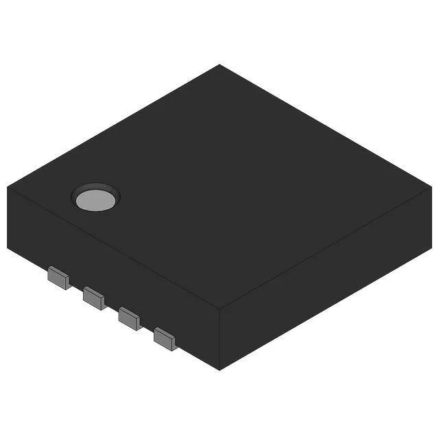
The differential output directly interfaces to modern high-speed ADCs with differential inputs, avoiding an external balun or transformer. That saves board area and removes the insertion loss and phase imbalance a transformer introduces. The common-mode output voltage can be set independently via the VOCM pin, which lets the designer match the ADC's common-mode input range without extra level-shifting resistors. The 8-WSON (2.5x3) package with exposed pad keeps the thermal path short for the 29.1 mA quiescent current plus load current.
The package is surface-mount only, so hand-assembly prototypes need a hot-air rework station with a fine nozzle.
Single-supply operation — what the voltage range allows
The 4.5 V to 12 V supply span covers both single-supply (5 V or 12 V) and split-supply (±2.25 V to ±6 V) configurations. In single-supply mode with a 5 V rail, the output common-mode can be set to 2.5 V via the VOCM pin, centering the differential swing within the ADC's input range. The input common-mode range for a current-feedback amplifier is typically limited — the datasheet's common-mode voltage range should be checked against the input signal's DC bias. For a ground-referenced input, a DC-blocking capacitor and bias network are needed.
For production BOMs, this means no near-term LTB risk. The NOPB suffix indicates a lead-free (NiPdAu) finish, RoHS-compliant, with no Pb in the plating.