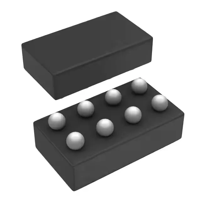
1:2 clock fanout in a 0.4 mm pitch BGA — what to know before layout
The Texas Instruments LMH2191TME/NOPB is a single-circuit, 1:2 fanout buffer for clock distribution. It takes one clock input and delivers two clock outputs, each rated up to 52 MHz. The part runs on a 2.5V to 5.5V supply rail, which covers both 3.3V and 5V logic families without a separate regulator. Both input and output are single-ended (non-differential), so this is a CMOS-level clock splitter, not an LVDS or LVPECL redriver. The 8-DSBGA package (0.4 mm pitch, no leads exposed) means the PCB fanout needs micro-vias or very fine trace escape — standard 0.5 mm pitch BGA rules don't apply.
Supply range and temperature — where it fits on the board
At 3.3V it's compatible with most MCU and FPGA clock outputs; at 5V it matches legacy TTL-level clock trees. No AEC-Q grade is cited, so it's not qualified for automotive under-hood use.
52 MHz ceiling — what it means for clock tree planning
52 MHz is the maximum frequency the outputs can cleanly reproduce. That's fast enough for most MCU clock inputs (48 MHz, 50 MHz, 25 MHz crystal oscillators), SPI bus distribution, and audio master clocks. It won't handle gigabit Ethernet reference clocks (125 MHz) or high-speed ADC sampling clocks above 50 MHz. For those, you need a differential fanout buffer rated above 100 MHz. The 1:2 ratio is fixed — one input fans to exactly two outputs, no enable or divider logic on-chip.
8-DSBGA — rework and inspection notes
The 8-WFBGA DSBGA is a wafer-level chip-scale package — 8 bumps, 0.4 mm pitch, no plastic overmold. The die is the package. That means: (1) solder joint inspection requires X-ray; (2) rework with hot air is possible but the die can crack if the profile exceeds 260°C peak; (3) underfill is recommended if the board sees vibration or thermal cycling; (4) the DSBGA version has no exposed thermal pad, so all heat dissipates through the solder balls into the PCB copper. The supplier device package is 8-DSBGA, which is the same physical footprint as the 8-WFBGA case code.