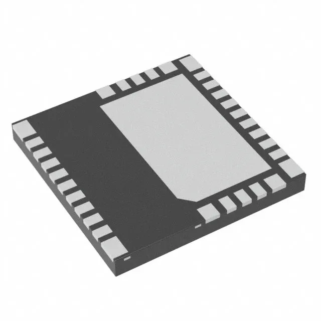
Texas Instruments LMG3411R070RWHT — Analog & Data Acquisition

LMG3411R070RWHT GaN FET with Integrated Driver, 70 mOhm

MPNLMG3411R070RWHT
End of Life

Texas Instruments LMG3411R070RWHT, 600-V 70-mOhm GaN FET with integrated driver, single high-side output, 12A max, 9.5V-18V supply, 32-VQFN Exposed Pad, -40 to 125°C.

$15.49Ref. price · indicative, final on quote
Packaging32-VQFN Exposed Pad
StockContact for availability
MOQ1 pcs
  • 100% new & originalTraceable channels only — no refurbs, no pulls, no remarked parts.
  • Date & lot codes on quoteStated per line before you commit; label photos on request.
  • MSL-compliant ESD packingMoisture-sealed bags with indicator cards; reels photo-verified.
  • PayPal buyer protectionPay by T/T, PayPal or Payoneer — card payments covered end to end.

Specifications

LMG3411R070RWHT Technical Specifications
ParameterValue
Input typeNon-Inverting
Output typeP-Channel
Switch typeLoad Switch
Mounting typeSurface Mount
Voltage - load480V (Max)
Voltage - supply (Vcc (Vdd))9.5V ~ 18V
Current - output12A
Number of outputs1
InterfaceLogic, PWM
Operating temperature-40°C ~ 125°C (TJ)
PackageTape & Reel (TR); Cut Tape (CT)
FeaturesBootstrap Circuit, 5V Regulated Output
Rds on70mOhm
Case32-VQFN Exposed Pad
Fault protectionOver Current, Over Temperature, UVLO
Output configurationHigh Side
Ratio - Input:Output1:1

Product details

GaN power stage with integrated driver — what the 70 mOhm Rds(on) means for the BOM

The Texas Instruments LMG3411R070RWHT is a 600 V GaN FET with an integrated gate driver, bootstrap circuit, and 5 V regulated output, all in a 32-VQFN Exposed Pad package. The headline 70 mOhm typical Rds(on) sets the conduction loss floor for a high-side load switch rated to 480 V maximum load voltage and 12 A continuous output. That Rds(on) figure is the number to size the heatsinking against: at 12 A the I²R loss hits about 10 W, so the exposed pad on the 32-VQFN (8x8 mm) needs a solid via-stitched thermal land on the PCB to keep junction temperature inside the -40 to 125 °C operating range. The integrated bootstrap and 5 V regulator eliminate the external bootstrap diode and a separate LDO for the high-side gate drive supply, pulling two to three passives off the BOM.

Protection set and supply rail requirements

The part integrates over-current, over-temperature, and UVLO fault protection, so a separate comparator-based protection circuit is not needed. The Vcc/Vdd supply range is 9.5 V to 18 V — design the bias rail for at least 10 V to hold margin through UVLO threshold. The PWM logic interface accepts a non-inverting input and drives a P-channel output configuration in a 1:1 input-to-output ratio. That means a single PWM signal from a controller or MCU directly controls the high-side switch; no level-shifter or dead-time generator is required because the integrated driver handles the bootstrap refresh.

Lifecycle and sourcing posture

For a BOM line that needs a GaN FET with integrated driver at this 70 mOhm / 480 V / 12 A rating, this is the current-production part to qualify.

Frequently asked questions

What is the Rds(on) of LMG3411R070RWHT?

The typical Rds(on) is 70 mOhm. That is the on-resistance at nominal operating conditions; the actual value shifts with junction temperature and gate drive voltage, but 70 mOhm is the number to use for first-pass conduction loss estimates.

What is the difference between LMG3411R070RWHT and other GaN FETs with integrated driver?

The key differentiator is the 70 mOhm Rds(on) at a 480 V load voltage rating, combined with the integrated bootstrap circuit and 5 V regulated output that reduce external BOM count. Many competing GaN parts require an external bootstrap diode or a separate 5 V supply for the driver. The 32-VQFN (8x8 mm) package with exposed pad is a standard footprint for this power level, so PCB layout migration from other 8x8 QFN GaN parts is usually straightforward.