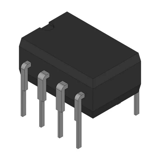
Texas Instruments LMC6042AIN — Logic ICs

LMC6042AIN CMOS Dual Op-Amp, 100 kHz, 0.02 V/µs Slew Rate

MPNLMC6042AIN
End of Life

Texas Instruments LMC6042AIN, CMOS dual operational amplifier, 100 kHz gain bandwidth, 0.02 V/µs slew rate, 26 µA supply per channel, rail-to-rail output, 8-DIP through-hole package, -40°C to 85°C.

$2.02Ref. price · indicative, final on quote
Packaging8-DIP (0.300", 7.62mm)
StockContact for availability
MOQ1 pcs
  • 100% new & originalTraceable channels only — no refurbs, no pulls, no remarked parts.
  • Date & lot codes on quoteStated per line before you commit; label photos on request.
  • MSL-compliant ESD packingMoisture-sealed bags with indicator cards; reels photo-verified.
  • PayPal buyer protectionPay by T/T, PayPal or Payoneer — card payments covered end to end.

Specifications

LMC6042AIN Technical Specifications
ParameterValue
Output typePush-Pull, Rail-to-Rail
Mounting typeThrough Hole
Amplifier typeCMOS
Voltage - input offset1 mV
Voltage - supply span15.5 V
Current - supply26µA (x2 Channels)
Current - input bias0.002 pA
Current - output (Channel)40 mA
Operating temperature-40°C ~ 85°C (TJ)
Gain bandwidth product100 kHz
PackageBulk
Slew rate0.02V/µs
Case8-DIP (0.300\", 7.62mm)
Number of circuits2

Product details

Micropower dual op-amp for low-frequency signal chains

The rail-to-rail output stage swings within millivolts of each supply rail, and the 0.002 pA input bias current lets it interface directly with high-impedance sources such as photodiode transimpedance stages, piezoelectric sensors, and electrochemical cell amplifiers without an external buffer. Supply range spans 4.5 V to 15.5 V, covering single 5 V and dual ±5 V rails as well as 12 V industrial supplies. The 8-DIP through-hole package (0.300" body, 7.62 mm pitch) is socket-friendly for prototyping and field-service replacement.

Slew rate and bandwidth — sizing for the signal

At 0.02 V/µs the LMC6042AIN is intentionally slow — that is the trade-off for the micropower supply current. For a 100 mV peak-to-peak output swing the amplifier can slew through the full transition in about 5 µs, which limits the useful small-signal bandwidth to roughly 3 kHz for a sine wave. This makes the part a natural fit for DC measurement, thermocouple conditioning, strain-gauge amplification, and low-frequency filter stages where the signal bandwidth stays below a few kilohertz. If the application needs to pass audio or switch faster than a few microseconds, a general-purpose op-amp with a 1 MHz to 10 MHz GBW and a 1 V/µs to 5 V/µs slew rate would be the correct class — but it would draw 10× to 50× the supply current.

Input bias current — direct sensor connection

The 0.002 pA (2 fA) typical input bias is among the lowest available in a dual CMOS op-amp. In a photodiode transimpedance amplifier with a 10 MΩ feedback resistor, that bias contributes just 20 nV of offset error — negligible compared to the 1 mV input offset voltage. For a pH probe or a high-impedance bridge, the bias current does not load the source, preserving accuracy. The CMOS input stage also keeps the input common-mode range within 0.3 V of the negative rail, so single-supply ground-referenced signals are handled without a negative rail.

Temperature grade and environment

The 8-PDIP package is not rated for high-vibration or sealed-environment applications where a surface-mount SOIC or TSSOP would be preferred, but it is well suited for benchtop instrumentation, lab equipment, and field-repairable control boards where socketed replacement is a design goal.

Output drive and rail-to-rail swing

The rail-to-rail output stage pulls within about 50 mV of the positive rail and within 10 mV of the negative rail at light loads, so the full supply range is usable for ADC drive or comparator thresholds. At 40 mA the output swing degrades — expect about 1.5 V from each rail — but for driving a 2 kΩ load the rail margin stays under 100 mV.

Lifecycle and sourcing

The part is RoHS non-compliant (lead-bearing), which limits its use in new EU RoHS-regulated designs but makes it a direct drop-in for legacy boards that require the tin-lead finish for solder-joint reliability or existing regulatory approvals.

Frequently asked questions

What are the typical applications for LMC6042AIN?

The LMC6042AIN is designed for low-frequency, micropower signal conditioning: photodiode transimpedance amplifiers, thermocouple and strain-gauge bridges, battery-monitoring circuits, portable instrumentation, and 4-20 mA loop-powered sensor interfaces where the 26 µA per channel supply current and 0.002 pA input bias are the key enablers.

Can LMC6042AIN be replaced with LMC6042AIM?

The LMC6042AIM is the surface-mount SOIC-8 variant of the same die — same electrical specs (100 kHz GBW, 0.02 V/µs slew rate, 26 µA supply, 0.002 pA input bias). The only difference is the package: the AIN is through-hole 8-DIP; the AIM is surface-mount SOIC-8. They are not pin-compatible on the same PCB footprint, but the electrical performance is identical.

What is the difference between LMC6042AIN and OPA4374AIPWT?

The OPA4374AIPWT is a quad CMOS op-amp with a 6.5 MHz gain-bandwidth and a 5 V/µs slew rate, drawing 600 µA per channel — roughly 23× the supply current per amplifier compared to the LMC6042AIN's 26 µA. The OPA4374 is a surface-mount TSSOP-14 part, not a through-hole DIP. If the design needs higher bandwidth and can tolerate the higher supply current, the OPA4374 is a functional alternative; for micropower applications the LMC6042AIN remains the correct choice.