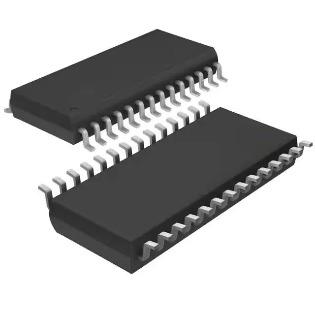
Texas Instruments DS90LV110TMTC/NOPB — Clock & Timing ICs

DS90LV110TMTC/NOPB Fanout Buffer, 1:10 LVDS, 400 MHz

MPNDS90LV110TMTC/NOPB
End of Life

Texas Instruments DS90LV110TMTC/NOPB, Fanout Buffer (Distribution), 1:10 LVDS, 400 MHz max, 3V-3.6V supply, -40°C to 85°C, 28-TSSOP.

$8.92Ref. price · indicative, final on quote
Packaging28-TSSOP (0.173", 4.40mm Width)
StockContact for availability
MOQ1 pcs
  • 100% new & originalTraceable channels only — no refurbs, no pulls, no remarked parts.
  • Date & lot codes on quoteStated per line before you commit; label photos on request.
  • MSL-compliant ESD packingMoisture-sealed bags with indicator cards; reels photo-verified.
  • PayPal buyer protectionPay by T/T, PayPal or Payoneer — card payments covered end to end.

Specifications

DS90LV110TMTC/NOPB Technical Specifications
ParameterValue
TypeFanout Buffer (Distribution)
Mounting typeSurface Mount
Voltage3V ~ 3.6V
Frequency400 MHz
Operating temperature-40°C ~ 85°C
InputLVDS, LVPECL, PECL
OutputLVDS
PackageTube
Case28-TSSOP (0.173\", 4.40mm Width)
Number of circuits1
Ratio - Input:Output1:10
Differential - Input:OutputYes/Yes

Product details

Clock fanout for LVDS, LVPECL, and PECL lines

The Texas Instruments DS90LV110TMTC/NOPB is a 1:10 fanout buffer that accepts LVDS, LVPECL, or PECL inputs and delivers ten LVDS outputs. It runs from a 3V to 3.6V supply and handles clock rates up to 400 MHz. The differential input and output path (Yes/Yes per the spec) preserves signal integrity across the fanout tree. This part sits in the clock distribution chain of telecom line cards, data-acquisition backplanes, and any system that needs to split a high-speed reference clock to multiple ASICs or FPGAs without degrading edge rates.

400 MHz ceiling and what it means for your line rate

The 400 MHz maximum frequency covers most LVDS clock distribution up to gigabit-class serial links (e.g., 1 GbE, SFP+ reference clocks). If your design needs to fan out a 312.5 MHz or 156.25 MHz oscillator to ten destinations, this buffer has the bandwidth. The 1:10 ratio means one device replaces two 1:5 or three 1:4 buffers, consolidating BOM count and routing complexity. However, the ten outputs present a combined load that the upstream clock source must drive — check the input capacitance and drive strength of the preceding PLL or oscillator.

Supply and temperature — 3.3V rail, industrial range

The 3V to 3.6V supply range ties this part to a 3.3V rail. If your board runs 2.5V or 5V clock logic, you will need a local regulator or a different buffer. The -40°C to 85°C operating temperature covers industrial environments — outdoor telecom cabinets, factory-floor controllers, and base stations. The 28-TSSOP package (0.173" body width, 4.40 mm) is a fine-pitch surface-mount footprint that routes well on standard PCB stacks.

Active lifecycle and compliance

It is ROHS3 compliant, which covers the EU RoHS exemption list. The NOPB suffix confirms lead-free construction — no Pb in the solder finish. For new designs, there is no imminent obsolescence risk.

Frequently asked questions

Is DS90LV110TMTC/NOPB RoHS compliant?

Yes, it is ROHS3 compliant per the lifecycle record. The NOPB suffix indicates lead-free construction.

What is the maximum frequency of DS90LV110?

The maximum frequency is 400 MHz. This covers most LVDS clock distribution up to gigabit serial link reference rates.

Is DS90LV110TMTC/NOPB compatible with 3.3V systems?

Yes, the supply range is 3V to 3.6V, so it runs directly on a 3.3V rail without an extra regulator.

What input and output signal types does this part support?

It accepts LVDS, LVPECL, or PECL inputs and delivers LVDS outputs. The differential path is maintained through the entire fanout tree.