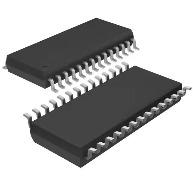
Texas Instruments DS90LV110ATMT/NOPB — Clock & Timing ICs

DS90LV110ATMT/NOPB Fanout Buffer, 1:10 LVDS, 200 MHz

MPNDS90LV110ATMT/NOPB
End of Life

Texas Instruments DS90LV110ATMT/NOPB, Fanout Buffer (Distribution), 1:10 input:output, 200 MHz max, LVDS/LVPECL/PECL input, LVDS output, 3V–3.6V supply, -40°C to 85°C, 28-TSSOP.

$9.61Ref. price · indicative, final on quote
Packaging28-TSSOP (0.173", 4.40mm Width)
StockContact for availability
MOQ1 pcs
  • 100% new & originalTraceable channels only — no refurbs, no pulls, no remarked parts.
  • Date & lot codes on quoteStated per line before you commit; label photos on request.
  • MSL-compliant ESD packingMoisture-sealed bags with indicator cards; reels photo-verified.
  • PayPal buyer protectionPay by T/T, PayPal or Payoneer — card payments covered end to end.

Specifications

DS90LV110ATMT/NOPB Technical Specifications
ParameterValue
TypeFanout Buffer (Distribution)
Mounting typeSurface Mount
Voltage3V ~ 3.6V
Frequency200 MHz
Operating temperature-40°C ~ 85°C
InputLVDS, LVPECL, PECL
OutputLVDS
PackageTube
Case28-TSSOP (0.173\", 4.40mm Width)
Number of circuits1
Ratio - Input:Output1:10
Differential - Input:OutputYes/Yes

Product details

200 MHz fanout buffer — one input drives ten LVDS loads

The Texas Instruments DS90LV110ATMT/NOPB is a 1:10 fanout buffer that accepts a single differential input — LVDS, LVPECL, or PECL — and distributes it as ten LVDS outputs. The 200 MHz maximum frequency sets the ceiling for clock or data distribution in systems like telecom backplanes, FPGA clock trees, and high-speed data-acquisition front ends. The 1:10 ratio means a single device can replace a two-stage buffer tree, saving board area and reducing additive jitter from cascaded stages. Supply range of 3V to 3.6V lets it run directly from a nominal 3.3V rail with margin for ripple and regulation tolerance. The industrial temperature range of -40°C to 85°C qualifies it for outdoor telecom enclosures, factory-floor automation, and other environments where the ambient can swing well past commercial limits. The 28-TSSOP package (4.40 mm body width) is a common footprint for clock distribution buffers; the surface-mount profile suits standard reflow assembly. Differential input and output paths throughout preserve signal integrity over the full temperature range.

Input flexibility — LVDS, LVPECL, or PECL accepted

The DS90LV110ATMT/NOPB accepts three common differential signalling standards on its single input: LVDS, LVPECL, and PECL. This cross-protocol compatibility is the part's main design-in advantage — it can sit between a PECL oscillator and an LVDS fanout tree, or buffer an LVPECL clock from an FPGA transceiver bank to multiple downstream LVDS receivers, without level-shifting resistors or a translator IC. The output is always LVDS, which keeps the fanout lanes at a consistent, low-swing standard that minimises EMI and power per link.

Active lifecycle — no LTB risk for new designs

The DS90LV110ATMT/NOPB carries an active product status from Texas Instruments. For a production BOM, this means the part can be specified into new designs without qualifying a substitute mid-lifecycle. The ROHS3 compliance covers current European and global material restrictions, so no separate Pb-free waiver is needed.

Frequently asked questions

What is the maximum operating frequency of DS90LV110ATMT/NOPB?

The DS90LV110ATMT/NOPB is rated for a maximum frequency of 200 MHz. This is the ceiling for the input clock or data signal; the ten LVDS outputs track the input rate up to that limit.

Is DS90LV110ATMT/NOPB RoHS compliant?

Yes, the DS90LV110ATMT/NOPB is ROHS3 compliant, meeting the latest European restriction-of-hazardous-substances requirements.