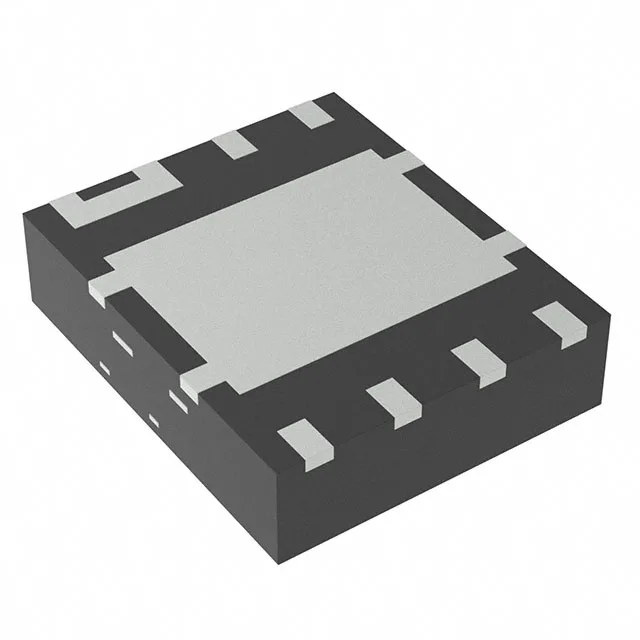
Half-bridge power stage in a single 8-LSON package
The Texas Instruments CSD86350Q5DT integrates two N-channel MOSFETs in a half-bridge configuration inside an 8-LSON (5x6) package. The high-side and low-side FETs have separate Rds(on) ratings: the high-side is 5 mOhm at 25 A and 5 V, the low-side is 1.1 mOhm at the same bias. That split is intentional — the low-side carries the inductor current during the freewheel period and sees higher duty-cycle conduction loss, so its lower resistance balances the thermal budget across the two dies. Gate charge is 10.7 nC for the high-side and 25 nC for the low-side at 4.5 V, and input capacitance is 1870 pF and 4000 pF respectively at 12.5 V. These numbers tell the gate-driver designer what the switching losses will look like and whether the driver can source enough peak current for the target frequency.
Store the reels dry; the LSON package is moisture-sensitive and needs a dry-bake if the moisture-barrier bag is breached.
The product status is Active and ROHS3 Compliant.