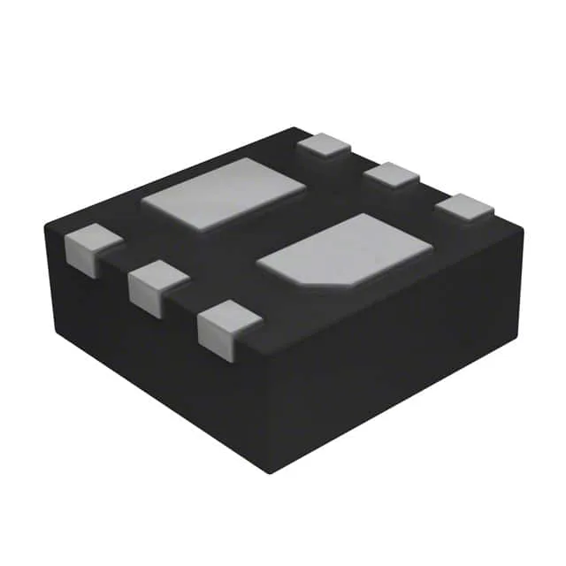
Texas Instruments CSD85301Q2

CSD85301Q2 NexFET Dual N-Ch MOSFET, 20V 5A, 27mOhm at 4.5V

MPNCSD85301Q2
End of Life

Texas Instruments NexFET™ series, CSD85301Q2, Dual N-Channel MOSFET, 20V Vdss, 5A Id, 27mOhm Rds(on) at 4.5V Vgs, Logic Level Gate, 6-WSON (2x2mm) package, -55°C to 150°C.

$0.67Ref. price · indicative, final on quote
Packaging6-WDFN Exposed Pad
StockContact for availability
MOQ1 pcs
  • 100% new & originalTraceable channels only — no refurbs, no pulls, no remarked parts.
  • Date & lot codes on quoteStated per line before you commit; label photos on request.
  • MSL-compliant ESD packingMoisture-sealed bags with indicator cards; reels photo-verified.
  • PayPal buyer protectionPay by T/T, PayPal or Payoneer — card payments covered end to end.

Specifications

CSD85301Q2 Technical Specifications
ParameterValue
SeriesNexFET™
FET type2 N-Channel (Dual)
Mounting typeSurface Mount
Drain to source voltage20V
Current - continuous drain (Id) @ 25°C5A
Power - max2.3W
Operating temperature-55°C ~ 150°C (TJ)
PackageTape & Reel (TR); Cut Tape (CT)
FET featureLogic Level Gate, 5V Drive
Case6-WDFN Exposed Pad
Vgs(th) (Max) @ id1.2V @ 250µA
Rds on (Max) @ id, vgs27mOhm @ 5A, 4.5V
Gate charge (Qg) (Max) @ vgs5.4nC @ 4.5V
Input capacitance (Ciss) (Max) @ vds469pF @ 10V

Product details

27 mOhm on-resistance at 4.5V — conduction loss floor

Maximum Rds(on) is 27 mOhm at Id=5A and Vgs=4.5V. This is the figure that sets the I²R conduction loss in a 5V-driven design. At 5A the dissipation is under 0.7W per channel, well within the 2.3W package power limit when the exposed pad is soldered to a suitable copper area. Gate charge is 5.4 nC max at 4.5V, and input capacitance Ciss is 469 pF at Vds=10V. These numbers keep the gate-drive energy low — a 5V GPIO from a microcontroller or a dedicated driver can switch the pair at moderate frequency without excessive crossover loss.

2x2 mm WSON with exposed pad — layout checklist

The 6-WSON package measures 2x2 mm with an exposed thermal pad. The 0.50 mm pitch is manageable on a two-layer board if the drain and source traces are kept wide enough for 5A. Operating junction temperature range is -55°C to 150°C. The 150°C ceiling gives headroom in high-ambient environments such as telecom enclosures or automotive cabin-adjacent modules, provided the thermal resistance of the board keeps the junction below the derating threshold at full load.

For a procurement desk qualifying a new BOM, this part does not carry the single-source risk that an NRND or EOL part would.

Frequently asked questions

What is the Rds(on) of CSD85301Q2 at 4.5V?

Maximum on-resistance is 27 mOhm at Id=5A and Vgs=4.5V. This is the worst-case figure for conduction-loss calculations at the rated current.

Is CSD85301Q2 compatible with 3.3V logic?

The gate threshold voltage Vgs(th) is 1.2V max at 250 µA, so the device will turn on with a 3.3V gate signal. However, the Rds(on) is specified at 4.5V Vgs; at 3.3V the on-resistance will be higher than the 27 mOhm max listed. For full rated performance, a 5V gate drive is recommended.

What is the replacement or equivalent for CSD85301Q2?

No official pin-compatible replacement or second-source alternate is listed on the record for this part. The CSD85301Q2 is a unique dual-NexFET in the 6-WSON 2x2 mm footprint. For a dual-sourcing strategy, a parametric search for dual N-channel MOSFETs in the same package with similar Rds(on) and Vdss ratings would be needed.