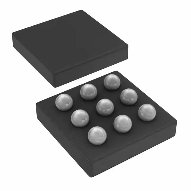
Texas Instruments CSD75207W15

CSD75207W15 NexFET Dual P-Channel MOSFET, 3.9A

MPNCSD75207W15
End of Life

Texas Instruments NexFET series, CSD75207W15, dual P-channel common-source MOSFET, 3.9A continuous drain, 162mOhm Rds(on) at 1.8V, logic-level gate, 700mW power dissipation, 9-DSBGA package, -55°C to 150°C junction temperature.

$0.68Ref. price · indicative, final on quote
Packaging9-UFBGA, DSBGA
StockContact for availability
MOQ1 pcs
  • 100% new & originalTraceable channels only — no refurbs, no pulls, no remarked parts.
  • Date & lot codes on quoteStated per line before you commit; label photos on request.
  • MSL-compliant ESD packingMoisture-sealed bags with indicator cards; reels photo-verified.
  • PayPal buyer protectionPay by T/T, PayPal or Payoneer — card payments covered end to end.

Specifications

CSD75207W15 Technical Specifications
ParameterValue
SeriesNexFET™
FET type2 P-Channel (Dual) Common Source
Mounting typeSurface Mount
Current - continuous drain (Id) @ 25°C3.9A
Power - max700mW
Operating temperature-55°C ~ 150°C (TJ)
PackageTape & Reel (TR); Cut Tape (CT)
FET featureLogic Level Gate
Case9-UFBGA, DSBGA
Vgs(th) (Max) @ id1.1V @ 250µA
Rds on (Max) @ id, vgs162mOhm @ 1A, 1.8V
Gate charge (Qg) (Max) @ vgs3.7nC @ 4.5V
Input capacitance (Ciss) (Max) @ vds595pF @ 10V

Product details

Dual P-Channel NexFET in a 9-DSBGA — what the 1.8V Rds(on) means

Its 162mOhm maximum Rds(on) at 1.8V gate drive and 1A drain current is the headline figure — it tells you this part is optimised for logic-level gate signals, not the 4.5V or 10V drives typical of standard P-channel parts. The 3.9A continuous drain rating at 25°C sets the load ceiling for a 9-DSBGA package that measures roughly 1.5mm per side, so the thermal path through the board copper is what actually governs the usable current in a real enclosure.

Gate charge and input capacitance — switching budget for a small footprint

The 3.7nC total gate charge at 4.5V and 595pF input capacitance at 10V drain bias are modest numbers that keep the switching losses low in a 500kHz to 1MHz buck or load-switch application. The logic-level gate threshold of 1.1V maximum at 250µA means the part turns on cleanly with a 1.8V GPIO — no level shifter needed between a 1.8V MCU output and the MOSFET gate.

Frequently asked questions

What is the Rds(on) of CSD75207W15 at 1.8V?

The maximum Rds(on) is 162mOhm at a 1.8V gate drive with 1A drain current. This is the rated condition — the on-resistance will be higher at lower gate voltages or elevated junction temperatures.

Can CSD75207W15 be used in a 1.8V logic level gate drive?

Yes. The logic-level gate threshold is 1.1V maximum at 250µA, and the Rds(on) is specified at 1.8V gate drive. A 1.8V GPIO from an MCU or SoC can drive the gate directly without a level shifter.